Active matrix substrate with TFT and capacitor, and LCD using the same

a technology of active matrix substrate and capacitor, which is applied in the direction of identification means, instruments, optics, etc., can solve the problems of reducing the effective pixel area, preventing and obtaining a valid pixel area as large as possible, so as to prevent the short circuit between the electrodes of the additional storage capacitor

Inactive Publication Date: 2007-01-02
JSR CORPORATIOON +1
View PDF14 Cites 17 Cited by
  • Summary
  • Abstract
  • Description
  • Claims
  • Application Information

AI Technical Summary

Benefits of technology

[0017]It is an object of the present invention to provide a thin film transistor substrate and a liquid crystal display that can prevent a short circuit between electrodes of an additional storage capacitor and obtain a larger valid pixel region at the same time.
[0018]It is another object of the present invention to provide a thin film transistor substrate and a liquid crystal display having a novel structure.
[0022]The short-circuiting between the electrodes of the additional storage capacitor can be prevented while obtaining a large valid area of the pixel electrode. A new structure of the thin film transistor and the liquid crystal display device are given.

Problems solved by technology

The additional storage capacitor is generally formed with an opaque body, and therefore causes a reduction in an effective pixel area.
In the thin film transistor substrate having an additional storage capacitor, preventing the short circuit between the electrodes of the additional storage capacitor and obtaining a valid pixel area as large as possible were difficult.

Method used


Image

  • Active matrix substrate with TFT and capacitor, and LCD using the same
  • Active matrix substrate with TFT and capacitor, and LCD using the same
  • Active matrix substrate with TFT and capacitor, and LCD using the same

Examples


Embodiment Construction

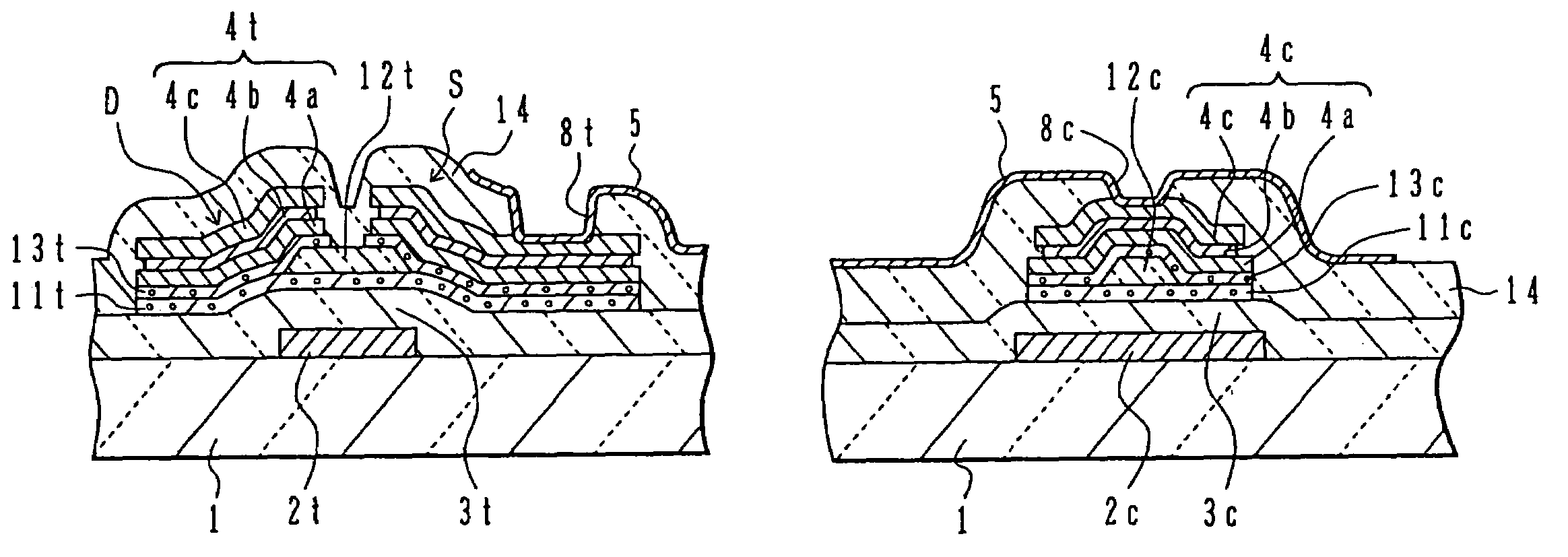
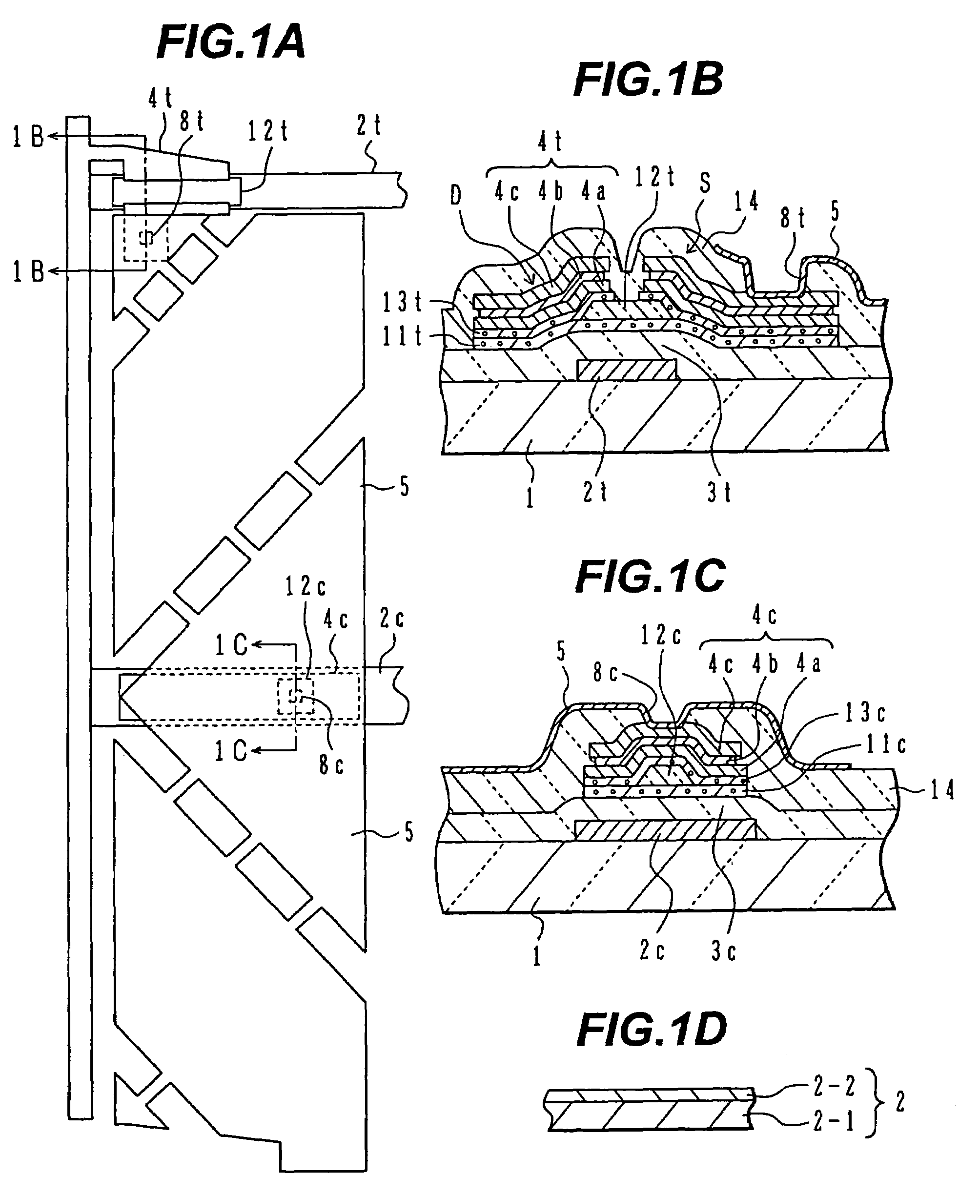
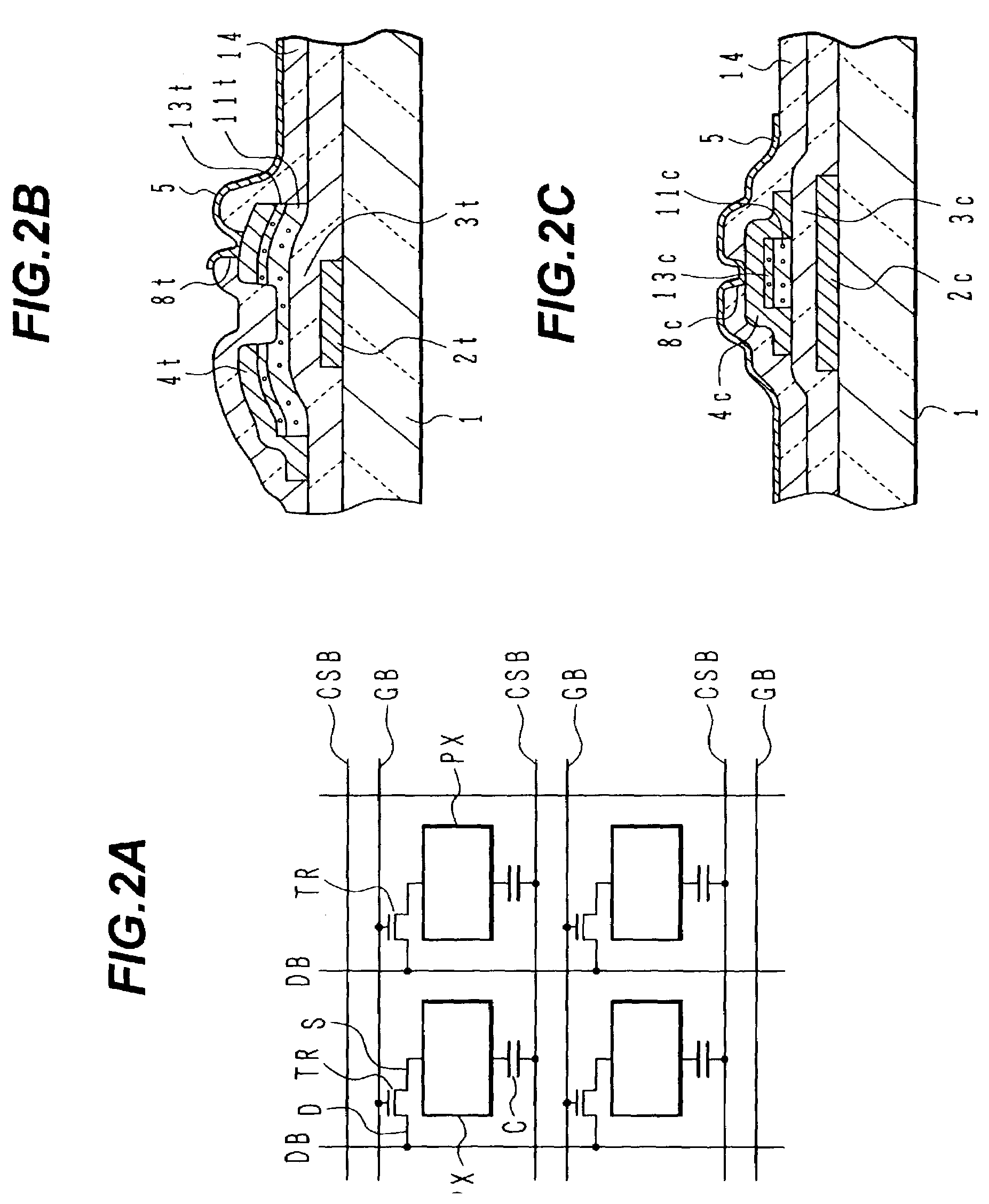
[0028]FIGS. 1A–1D are a plan view and cross-sectional views showing a structure of a thin film transistor (TFT) substrate according to an embodiment of this invention. FIG. 1B is a cross sectional view showing the thin film transistor region along a line IB—IB in FIG. 1A, and FIG. 1C is a cross sectional view showing an additional or auxiliary storage capacitor region along a line IC—IC in FIG. 1A.

[0029]A gate bus line 2t and an additional storage capacitor bus line 2c are formed on the glass substrate 1 by depositing an electrode layer, for example by sputtering a layer, and patterning the layer by photolithography. A transparent substrate is used for a transparent liquid crystal display. An opaque substrate other than a transparent substrate can be used for a reflective liquid crystal display, although the surface should be insulated. A substrate having an insulating surface, for example a silicon substrate with an oxide film, a metal plate having an insulating layer on the surfac...


PUM

PropertyMeasurementUnit
thicknessaaaaaaaaaa
thicknessaaaaaaaaaa
thicknessaaaaaaaaaa

Abstract

A thin-film transistor substrate, including a substrate with an insulating surface, gate electrodes, lower electrodes of capacitors made of the same material layer as the gate electrodes, a first insulating layer, a channel layer of high resistivity semiconductor having a concave part, and a pair of low resistivity source / drain electrodes. There is also a second insulating layer formed on the first insulating layer. A first connection hole penetrates the second insulating layer and exposes one of each of the pair of the source / drain electrodes. A second connection hole penetrates the second insulating layer and exposes a connection region of each of the upper layers of the upper electrode above the lower layer. A pixel electrode is formed on the second insulating layer and is connected to one of the source / drain electrodes and the upper layer of the upper electrode of the capacitor via the first and second connection holes.

Description

CROSS REFERENCE TO RELATED APPLICATION[0001]This application is based on Japanese Patent Application 2001-387961, filed on Dec. 20, 2001, the entire contents of which are incorporated herein by reference.BACKGROUND OF THE INVENTION[0002]A) Field of the Invention[0003]This invention relates to a thin film transistor (TFT) substrate and a liquid crystal display and especially to those having additional or subsidiary storage capacitors.[0004]B) Description of the Related Art[0005]Recently, a liquid crystal display is widely used for an information device, etc., and lower cost and higher resolution are sought. Most of thin film transistor substrates have additional or subsidiary storage capacitors for storing information for pixel electrodes at respective pixels. The additional storage capacitor is generally formed with an opaque body, and therefore causes a reduction in an effective pixel area. Miniaturization of the additional storage capacitor that occupies a comparatively large regi...

Claims


Application Information

Patent Timeline
Patent Type & Authority Patents(United States)
IPC IPC(8): H01L29/04H01L31/036H01L31/0376H01L31/20G02F1/1333G02F1/1368G02F1/1343G02F1/1362G09F9/30H01L21/28H01L21/336H01L21/768H01L27/12H01L29/786
CPCG02F1/136213H01L29/78669H01L29/66765H01L29/78621H01L27/12G02F1/136227
Inventor FUJIKAWA, TETSUYADOI, SEIJI
Owner JSR CORPORATIOON
Why Eureka
Try Eureka