
Electronic device

a piezoelectric film and electronic technology, applied in the field of electronic devices, can solve the problems of affecting the characteristics of film bulk acoustic resonators, degrading q-value at resonance frequency, increasing resistance and eventually disconnection

Inactive Publication Date: 2007-12-13
KK TOSHIBA
View PDF15 Cites 78 Cited by
  • Summary
  • Abstract
  • Description
  • Claims
  • Application Information

AI Technical Summary

Problems solved by technology

It turns out from these investigations that the increase of the series resistance of the electrode due to the above selection of material causes degradation in Q-value at resonance frequency and greatly affects the characteristics of the film bulk acoustic resonator.
However, unfortunately, nickel-rich alloys have high specific resistance, and suffer from microcracks due to residual stress, resulting in increased resistance and eventually, disconnection.
However, unfortunately, the melting point of Al is as low as about 660° C., and hence hillocks and voids are likely to occur in the process of forming a piezoelectric film under the influence of thermal hysteresis.

Method used


Image

  • Electronic device
  • Electronic device
  • Electronic device

Examples


Embodiment Construction

[0027] An embodiment of the invention will now be described with reference to the drawings.

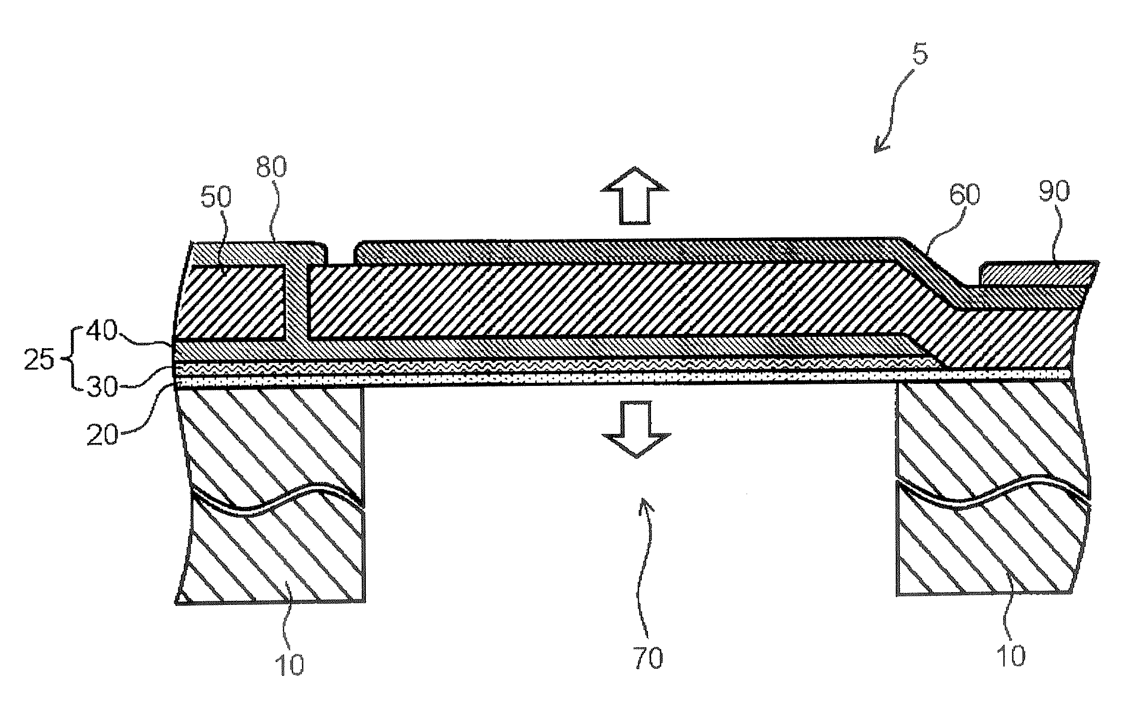
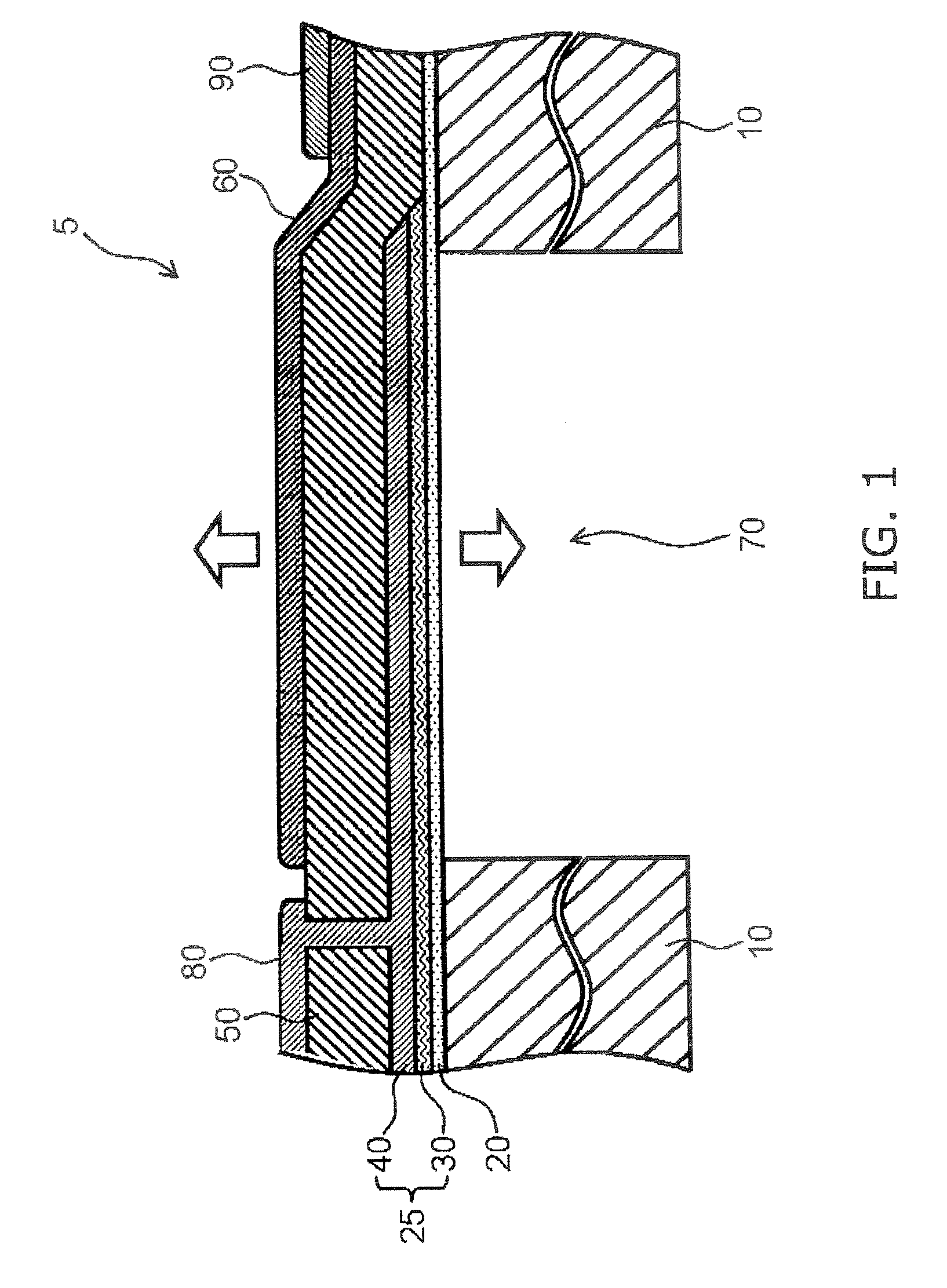
[0028]FIG. 1 is a schematic cross-sectional view showing an electronic device according to a first example of the invention.

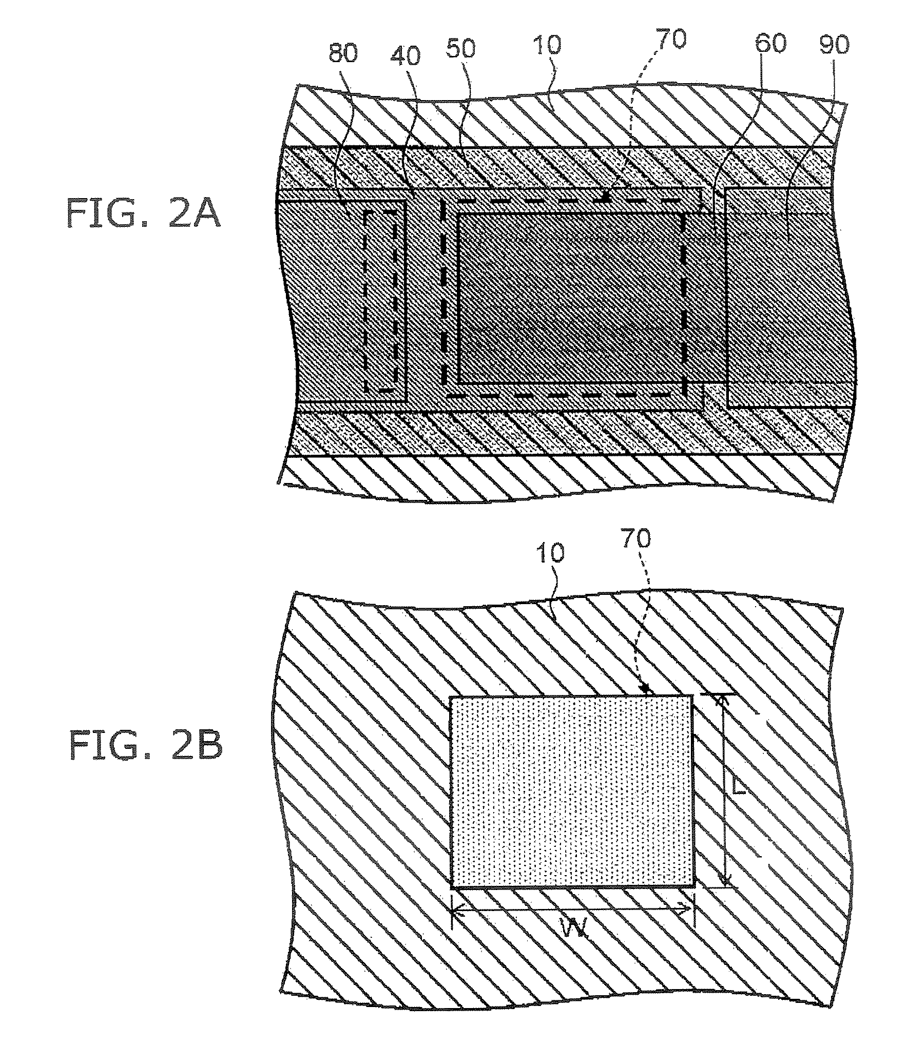
[0029]FIGS. 2A and 2B are a top view and a bottom view of the electronic device of this example, respectively. With regard to FIG. 2 and the following figures, elements similar to those described earlier are marked with the same reference numerals and not described in detail.

[0030] The electronic device of this embodiment is a film bulk acoustic resonator or bulk acoustic wave (BAW) device 5. This BAW device 5 is formed on a support substrate 10 of e.g. silicon (Si). The support substrate 10 has a hollow portion (cavity) 70. On the entire surface of the support substrate 10 is provided a passivation layer 20 of e.g. thermal oxide film (SiNx). A laminated electrode film 25 is provided on the passivation layer 20. The laminated electrode film 25 has a structure in which,...


PUM

PropertyMeasurementUnit
melting pointaaaaaaaaaa
thicknessaaaaaaaaaa
thicknessaaaaaaaaaa

Abstract

An electronic device includes: a lower electrode; a first piezoelectric film provided on the lower electrode; and an upper electrode provided on the first piezoelectric film. At least one of the lower electrode and the upper electrode is made of an alloy composed primarily of aluminum and doped with at least one element selected from the group consisting of Ni, Co, V, Ta, Mo, W, Ti, Y, and Nd. Alternatively, an electronic device includes: a support substrate; a lower electrode provided on the support substrate; a first piezoelectric film provided on the lower electrode; and an upper electrode provided on the first piezoelectric film. The lower electrode is made of an alloy composed primarily of aluminum and doped with at least one element selected from the group consisting of Ni, Co, V, Ta, Mo, W, Ti, Y, and Nd.

Description

CROSS-REFERENCE TO RELATED APPLICATIONS [0001] This application is based upon and claims the benefit of priority from the prior Japanese Patent Application No. 2006-162552, filed on Jun. 12, 2006; the entire contents of which are incorporated herein by reference. BACKGROUND OF THE INVENTION [0002] 1. Field of the Invention [0003] This invention relates to an electronic device, and more particularly to an electronic device having a piezoelectric film such as a film bulk acoustic resonator and a MEMS device. [0004] 2. Background Art [0005] Recently, MEMS (Micro-Electro-Mechanical System) devices with an acceleration sensor or a pressure sensor integrated on a silicon substrate, as well as film bulk acoustic resonators (FBARs) or bulk acoustic wave (BAW) devices have been developed, and are promising for practical use. [0006] For example, BAW devices are expected to be installed in RF antenna filters for gigahertzband W-CDMA and duplexers for mobile information terminals. The main part...

Claims


Application Information

Patent Timeline
Patent Type & Authority Applications(United States)
IPC IPC(8): H01L41/047H01L41/09H01L41/18H01L41/187H01L41/22H01L41/29H03H9/17
CPCH01L41/047H03H9/02094H03H9/13H03H9/131H03H9/173H01L41/0973H04R17/02H04R19/04H04R2201/003H01L41/094H03H9/174H10N30/877H10N30/2042H10N30/2047
Inventor SANO, KENYAYANASE, NAOKOOHARA, RYOICHIYASUMOTO, TAKAAKI
Owner KK TOSHIBA
Features
  • Generate Ideas
  • Intellectual Property
  • Life Sciences
  • Materials
  • Tech Scout
  • Unparalleled Data Quality
  • Higher Quality Content
  • 60% Fewer Hallucinations
Learn More