Semiconductor memory device

a memory device and semiconductor technology, applied in static storage, digital storage, instruments, etc., can solve the problems of reducing the write speed and therefore increasing the write time, affecting the write speed, so as to achieve the effect of decentralizing the write operation

Active Publication Date: 2007-12-13
KIOXIA CORP
View PDF7 Cites 157 Cited by
  • Summary
  • Abstract
  • Description
  • Claims
  • Application Information

AI Technical Summary

Benefits of technology

[0011]According to a second aspect of the invention, there is provided a semiconductor memory device comprising: a memory cell array which include a first region that has a plurality of memory cells each capable of storing n-bit data (n is a natural number) and a second region that has a plurality of memory cells each capable of storing k-bit data (k>n: k is a natural number); a data storage circuit which includes a plurality of data caches; and a control circuit which controls the memory cell array and the data storage circuit so as to decentralize write operations by specifying an address in the memory cell array to prevent write operations from concentrating on a specific one of the memory cells.

Problems solved by technology

However, the data write time of the multilevel NAND flash memory has to be, for example, about two to three times that of the single-level NAND flash memory, which is disadvantageous to speeding up.
To perform control so as to make the distribution width of the threshold voltage narrower, it is necessary to repeat a program and a program verify read operation, which decreases the write speed and therefore increases the write time.
For this reason, to store more items of data, it is necessary to make the distribution of threshold voltages narrower, making the write speed much slower, which is disadvantageous to speeding up.
However, only one bit of data can be stored in a single memory, which is disadvantageous to making the capacity larger.

Method used


Image

  • Semiconductor memory device
  • Semiconductor memory device
  • Semiconductor memory device

Examples


first embodiment

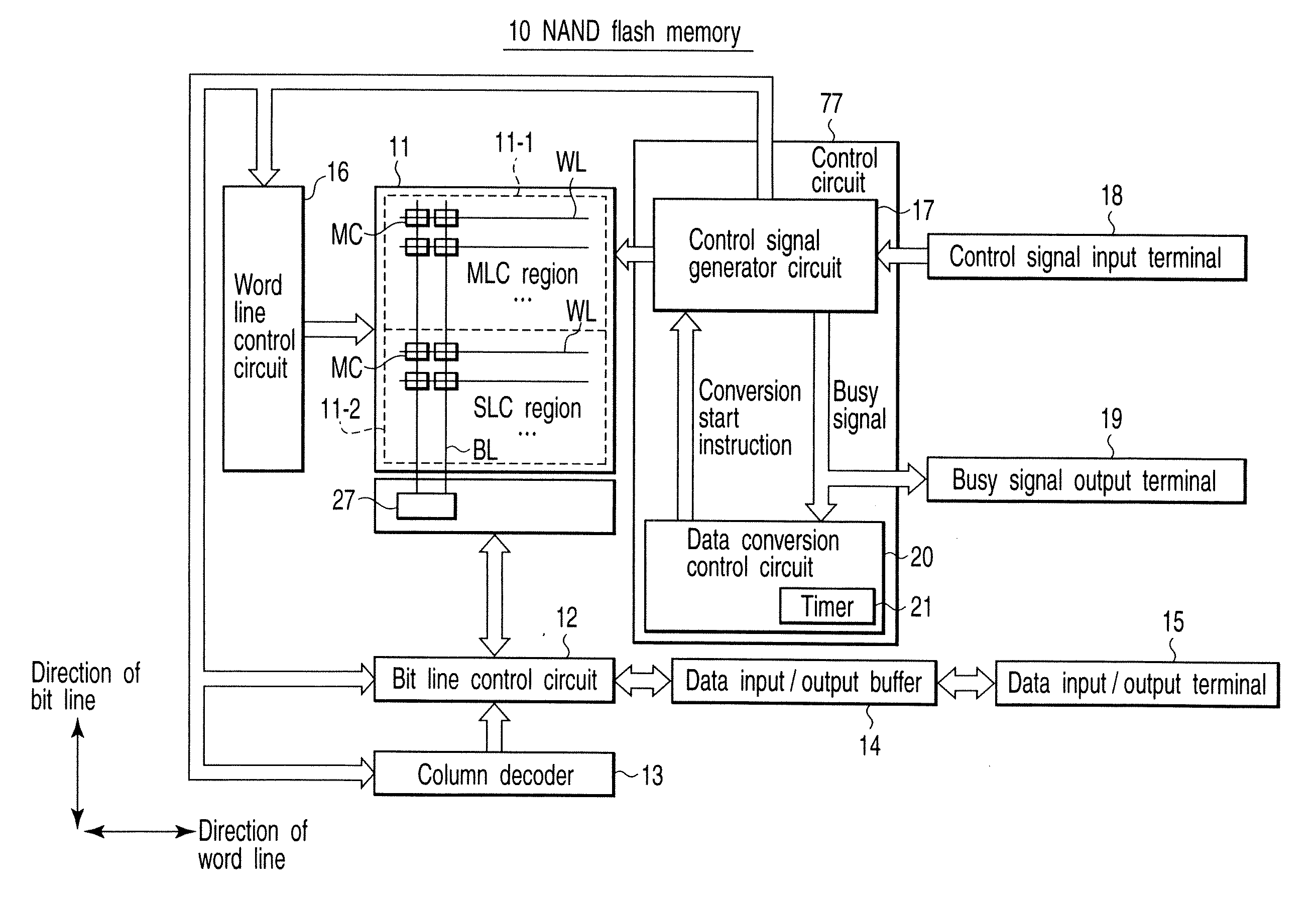
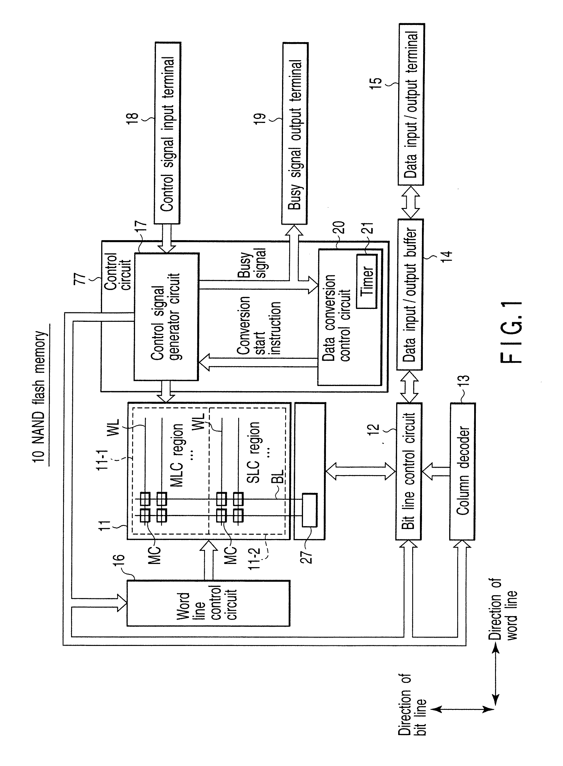
[0034]Using FIGS. 1 to 14, a semiconductor memory device according to a first embodiment of the invention will be explained. FIG. 1 is a block diagram of a semiconductor memory device according to the first embodiment. In the embodiment, a NAND flash memory is taken as an example.

[0035]As shown in FIG. 1, the NAND flash memory 10 comprises a memory cell array 11, a data storage circuit 27, a bit line control circuit 12, a column decoder 13, a data input / output buffer 14, a data input / output terminal 15, a word line control circuit 16, a control signal input terminal 18, a busy signal output terminal 19, and a control circuit 77 which has a control signal generator circuit 17 and a data conversion control circuit 20.

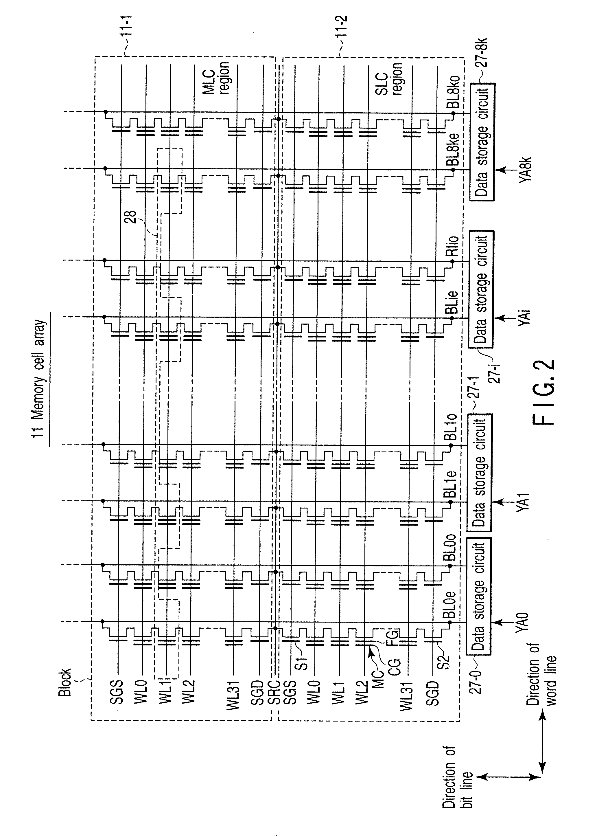
[0036]The memory cell array 11 includes an MLC (Multi Level Cell) region 11-1 which has as memory cells MC multilevel NAND flash memories capable of recording a plurality of bits of data into a single memory and an SLC (Single Level Cell) region 11-2 which has as memory c...

second embodiment (

Example of Providing a Controller)

[0140]Next, using FIG. 18, a semiconductor memory device according to a second embodiment of the invention will be explained. FIG. 18 is a block diagram of a semiconductor memory device according to the second embodiment. The second embodiment relates to an example of further providing a controller 50. In the description below, a detailed explanation of the parts overlapping with those in the first embodiment will be omitted.

[0141]As shown in FIG. 18, the semiconductor memory device according to the second embodiment differs from the first embodiment in the following points.

[0142]The semiconductor memory device of the second embodiment further includes a controller 50. Moreover, the second embodiment differs from the first embodiment in that the NAND flash memory 10 does not have the data conversion control circuit 20.

[0143]The controller 50 is configured to manage the physical state of the inside of the NAND flash memory 10 (for example, in what bl...

third embodiment (

Example of Providing an SLC Region / MLC Region Defining Circuit)

[0150]Next, using FIG. 19, a semiconductor memory device according to a third embodiment of the invention will be explained. FIG. 19 is a block diagram of a semiconductor memory device according to the third embodiment. The third embodiment relates to an example of further providing an SLC region / MLC region defining circuit. In the description below, a detailed explanation of the parts overlapping with those in the first embodiment will be omitted.

[0151]As shown in FIG. 19, the semiconductor memory device differs from that of the first embodiment in that the control signal generator circuit 17 includes an SLC region / MLC region defining circuit 79.

[0152]The SLC region / MLC region defining circuit 79 is configured to define either the SLC region 11-2 or MLC region 11-1 in each block, a region in the memory cell array 11.

[0153]Therefore, for example, when an instruction to the effect that “Do writing in the SLC region 11-2” ...


PUM


Abstract

A semiconductor memory device of the invention comprises a memory cell array which includes a first region that has a plurality of memory cells each capable of storing n-bit data (n is a natural number) and a second region that has a plurality of memory cells each capable of storing k-bit data (k>n: k is a natural number), a data storage circuit which includes a plurality of data caches, and a control circuit which controls the memory cell array and the data storage circuit in such a manner that the k-bit data read from the k / n number of memory cells in the first region are stored into the data storage circuit and the k-bit data are stored into the memory cells in the second region.

Description

CROSS-REFERENCE TO RELATED APPLICATIONS[0001]This application is based upon and claims the benefit of priority from prior Japanese Patent Application No. 2006-131800, filed May 10, 2006, the entire contents of which are incorporated herein by reference.BACKGROUND OF THE INVENTION[0002]1. Field of the Invention[0003]This invention relates to a semiconductor memory device, and more particularly to a semiconductor memory device applied to, for example, a NAND flash memory.[0004]2. Description of the Related Art[0005]NAND flash memories, semiconductor memory devices, have been available in the market and widely used. The NAND flash memories come in two types: one is a single-level NAND flash memory capable of storing 1 bit of data in a single memory cell and the other is a multilevel NAND flash memory capable of storing a plurality of pieces of data in a single memory cell (refer to, for example, Jpn. Pat. Appln. KOKAI Publication No. 2002-016154).[0006]Since a multilevel NAND flash mem...

Claims


Application Information

Patent Timeline
Patent Type & Authority Applications(United States)
IPC IPC(8): G11C11/34
CPCG11C11/5628G11C16/0483G11C2211/5643G11C2211/5641G11C16/12G11C16/00
Inventor SHIMIZU, TAKAHIROSHIBATA, NOBORU
Owner KIOXIA CORP
Why Eureka
Try Eureka