Method of Manufacturing an Array Substrate of a Transflective Liquid Crystal Display

a liquid crystal display and array substrate technology, applied in the direction of electrical equipment, semiconductor devices, instruments, etc., can solve the problems of the highest production cost of the lithography process, achieve the effect of reducing the number of photo-masks needed, increasing the capacitance value per unit of area, and reducing the number of photo-masks

Active Publication Date: 2007-12-13
AU OPTRONICS CORP
View PDF7 Cites 13 Cited by
  • Summary
  • Abstract
  • Description
  • Claims
  • Application Information

AI Technical Summary

Benefits of technology

[0012]In according to the present invention, half-tone photo-masks and back exposures are used to reduce the number of photo-masks needed in the lithography process. Therefore, only three to four photo-masks are needed in manufacturing a transflective LCD. Besides, The storage capacitances connect in series, not only the capacitance value per unit of area can be increased but also the overall area on the substrate occupied by the storage capacitance can be reduced. Moreover, the aperture rate of the penetrating region of the pixel region and the brightness of the LCD are increased.

Problems solved by technology

Among these processes, the lithography process has the highest production cost.

Method used


Image

  • Method of Manufacturing an Array Substrate of a Transflective Liquid Crystal Display
  • Method of Manufacturing an Array Substrate of a Transflective Liquid Crystal Display
  • Method of Manufacturing an Array Substrate of a Transflective Liquid Crystal Display

Examples


first embodiment

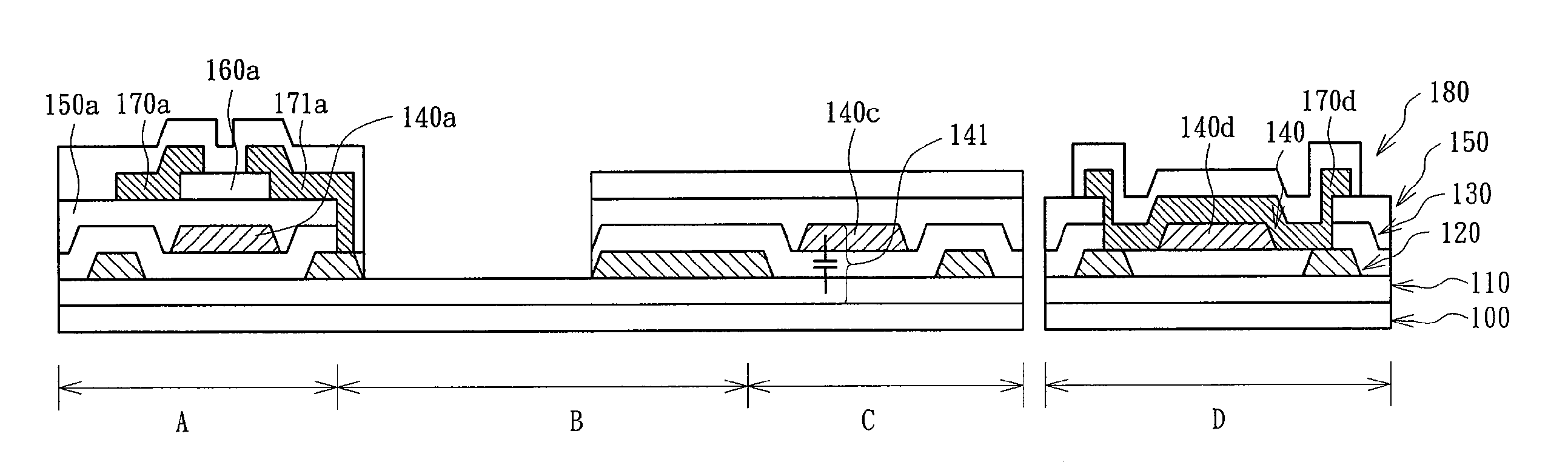
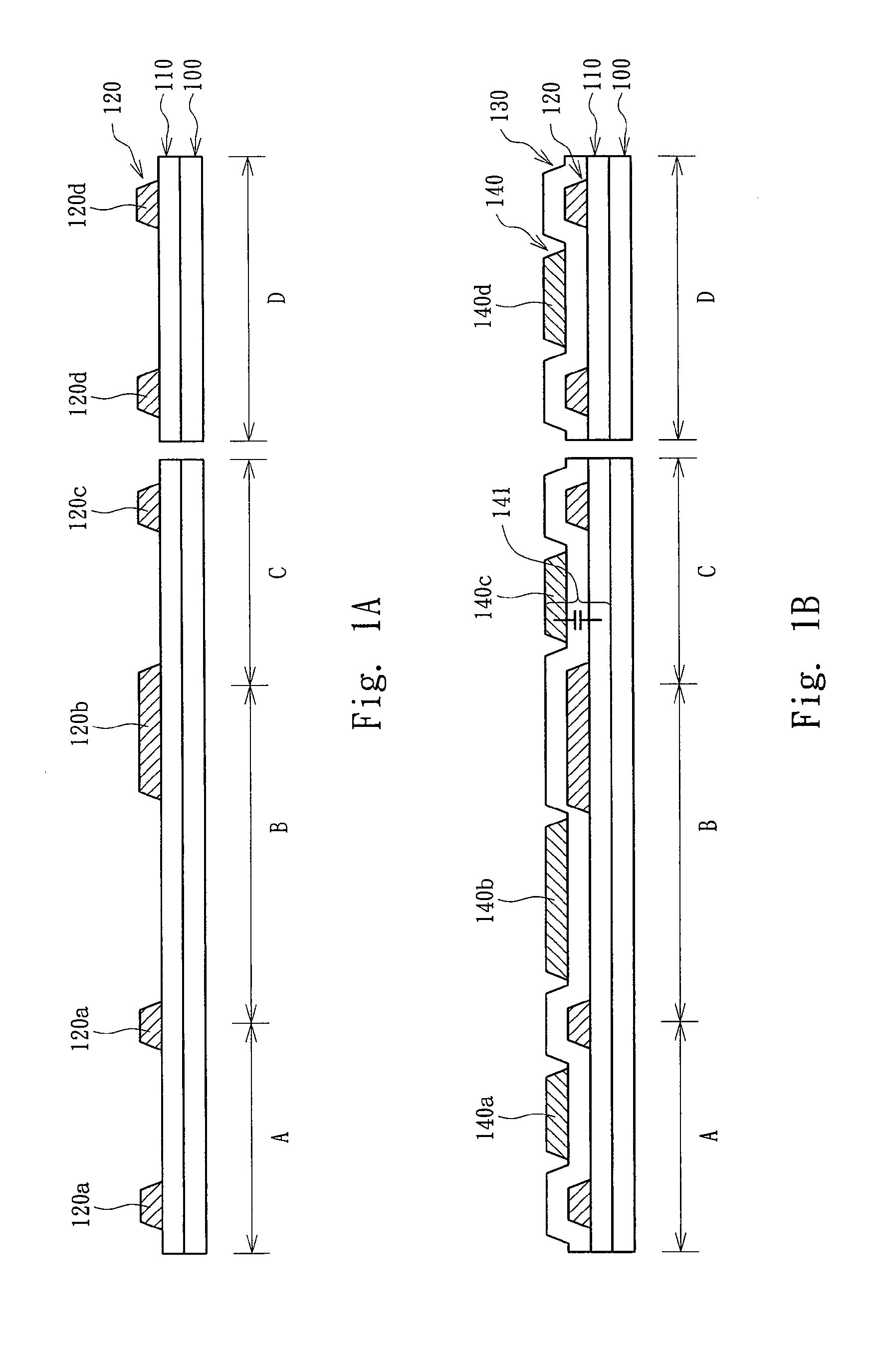
[0016]FIGS. 1A-1G are cross-section views of an array substrate of a transflective LCD in process steps according to the first embodiment of the present invention. In FIG. 1A, regions from left to right are a thin film transistor (TFT) region A, a pixel region B, a storage capacitance region C and a gate pad region D, respectively. First, a transparent conductive layer 110 and a fist metal layer 120 are formed sequentially on a substrate 100. Then, a first half-tone photo-mask is used to define the first metal layer 120 and the transparent conductive layer 110 simultaneously. The first metal layer 120 is defined to form complementary patterns 120a, 120c and 120d and a reflective layer 120b, which is on a penetrating portion of the pixel region B. The complementary patterns 120a, 120c and 120d are the complementary patterns of a gate electrode, a capacitance line and a gate pad, respectively. A complementary pattern of a scan line is also formed in the first metal layer 120 but not s...

second embodiment

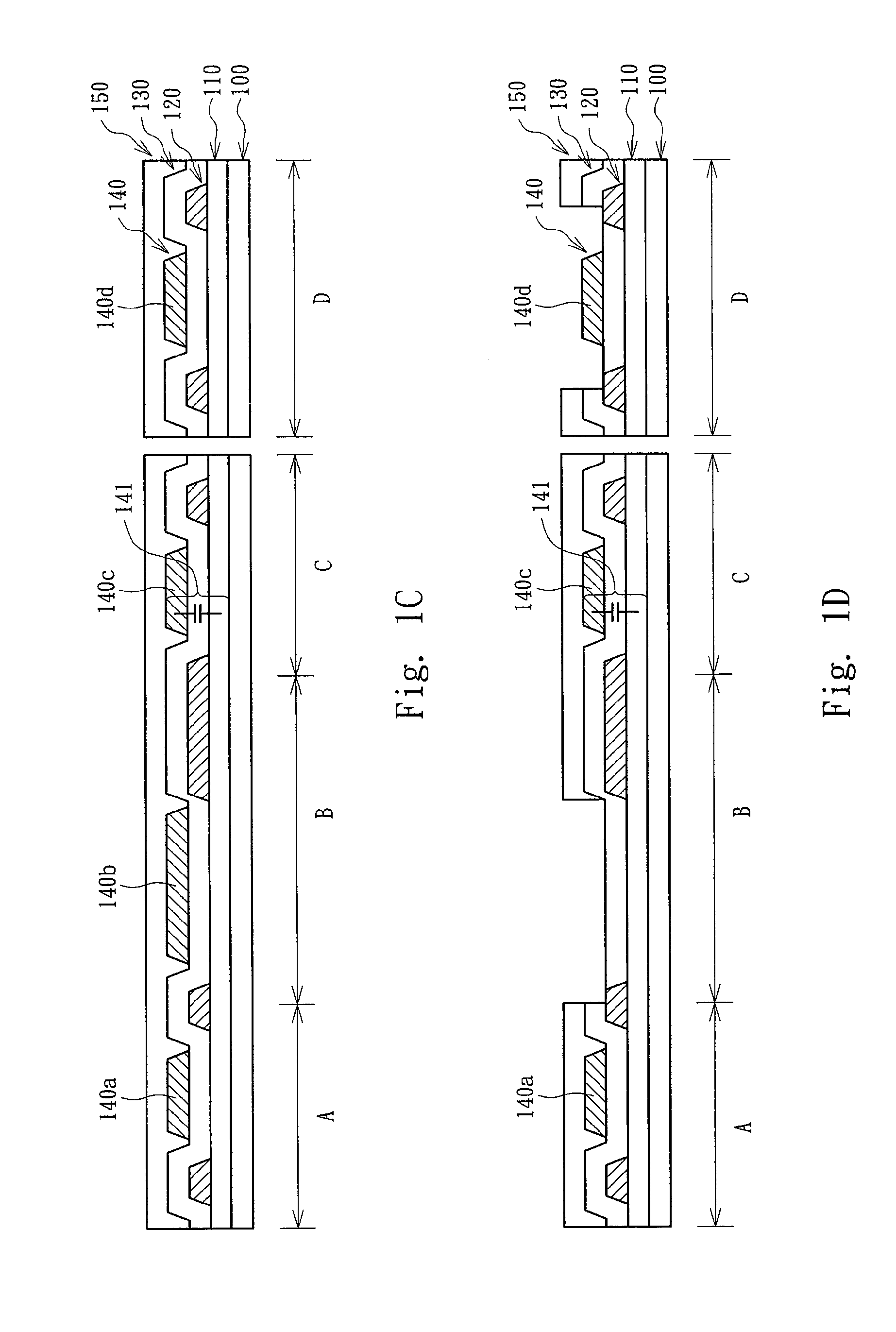
[0024]FIGS. 2A-2D are cross-section views of an array substrate of a transflective LCD in process steps according to the second embodiment. From the process step of forming the transparent conductive layer 110 to the process step of forming the dielectric layer 150, the second embodiment is the same as the first embodiment. Therefore, the description about these process steps can be directly referred to the first embodiment.

[0025]In FIG. 2A, a second photo-mask is used to define the dielectric layer 150, the second metal layer 140 and the first passivation layer 130 after forming the dielectric layer 150. In this process step, the sacrifice metal layer 140b on the penetrating portion of the pixel region B and the dielectric layer 150 thereon are removed, at the same time, the dielectric layer 150 and the first passivation layer 130 on a side of the first storage capacitance 141 is removed to form a contact window 151. Moreover, the dielectric layer 150 and the first passivation laye...


PUM


Abstract

A method of manufacturing an array substrate of a transflective liquid crystal display is provided. Utilizing backward exposure and half-tone photo-mask to reduce the number of photo-masks used in the manufacturing process, only three to four photo-masks are used to manufacture a transflective liquid crystal display.

Description

RELATED APPLICATIONS[0001]The present application is based on, and claims priority from, Taiwan Application Serial Number 95121086, filed Jun. 13, 2006, the disclosure of which is hereby incorporated by reference herein in its entirety.BACKGROUND[0002]1. Field of Invention[0003]The present invention relates to a method of manufacturing an array substrate of a liquid crystal display (LCD). More particularly, the present invention relates to a method of manufacturing an array substrate of a transflective LCD.[0004]2. Description of Related Art[0005]Recently, the progress of opto-electronic technology and the rapid development of digital technology push forward the expansion of the LCD market. Because the LCD has many advantages such as high display quality, small size, light weight, low driving voltage and low power consumption, it has been widely applied to many electronics products such as PDAs, mobile phones, digital videos, notebooks, desk-top displays, digital cameras and project...

Claims


Application Information

Patent Timeline
Patent Type & Authority Applications(United States)
IPC IPC(8): H01L21/84
CPCH01L27/1288H01L27/1255G02F1/13G02F1/1335G02F1/136
Inventor LIN, SHIH-CHIEH
Owner AU OPTRONICS CORP
Why Eureka
Try Eureka