Magnetic sensor and method for detecting magnetic field

a magnetic field and sensor technology, applied in the direction of galvano-magnetic devices, instruments, magnetic measurements, etc., can solve the problems of unbalance voltage and unbalance of electric potential distribution, and achieve the effect of reducing the offset voltage of the sensor

Inactive Publication Date: 2007-12-20
DENSO CORP
View PDF2 Cites 110 Cited by
  • Summary
  • Abstract
  • Description
  • Claims
  • Application Information

AI Technical Summary

Benefits of technology

[0014] In the above method, the Hall voltage is detected by switching the first and second electrodes between a driving current supply electrode and a Hall voltage detecting electrode so that an offset voltage of the sensor is reduced.

Problems solved by technology

Accordingly, an unbalance of an electric potential distribution is caused by an influence such as an alignment shift, the shape of an element, etc., and an offset voltage (unbalance voltage) is easily caused.

Method used


Image

  • Magnetic sensor and method for detecting magnetic field
  • Magnetic sensor and method for detecting magnetic field
  • Magnetic sensor and method for detecting magnetic field

Examples


first embodiment

Mode

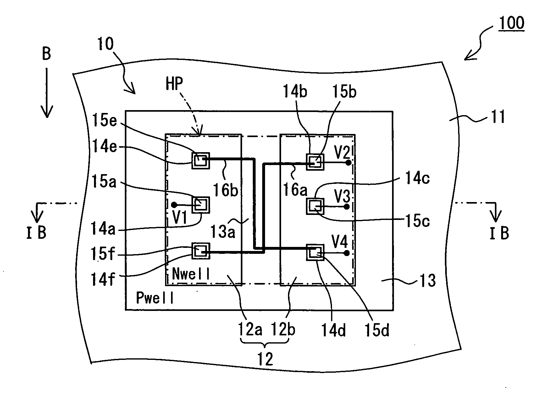
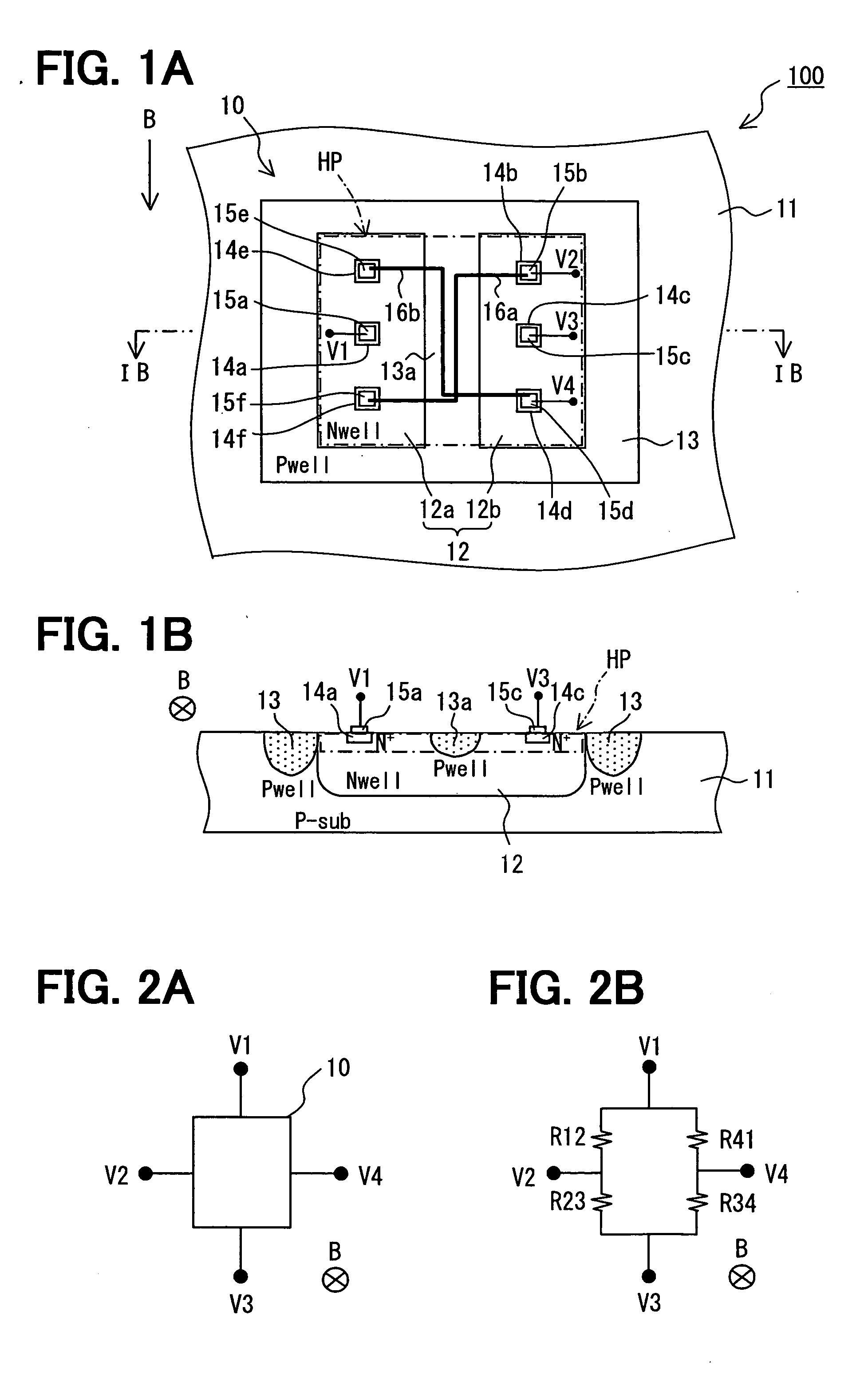
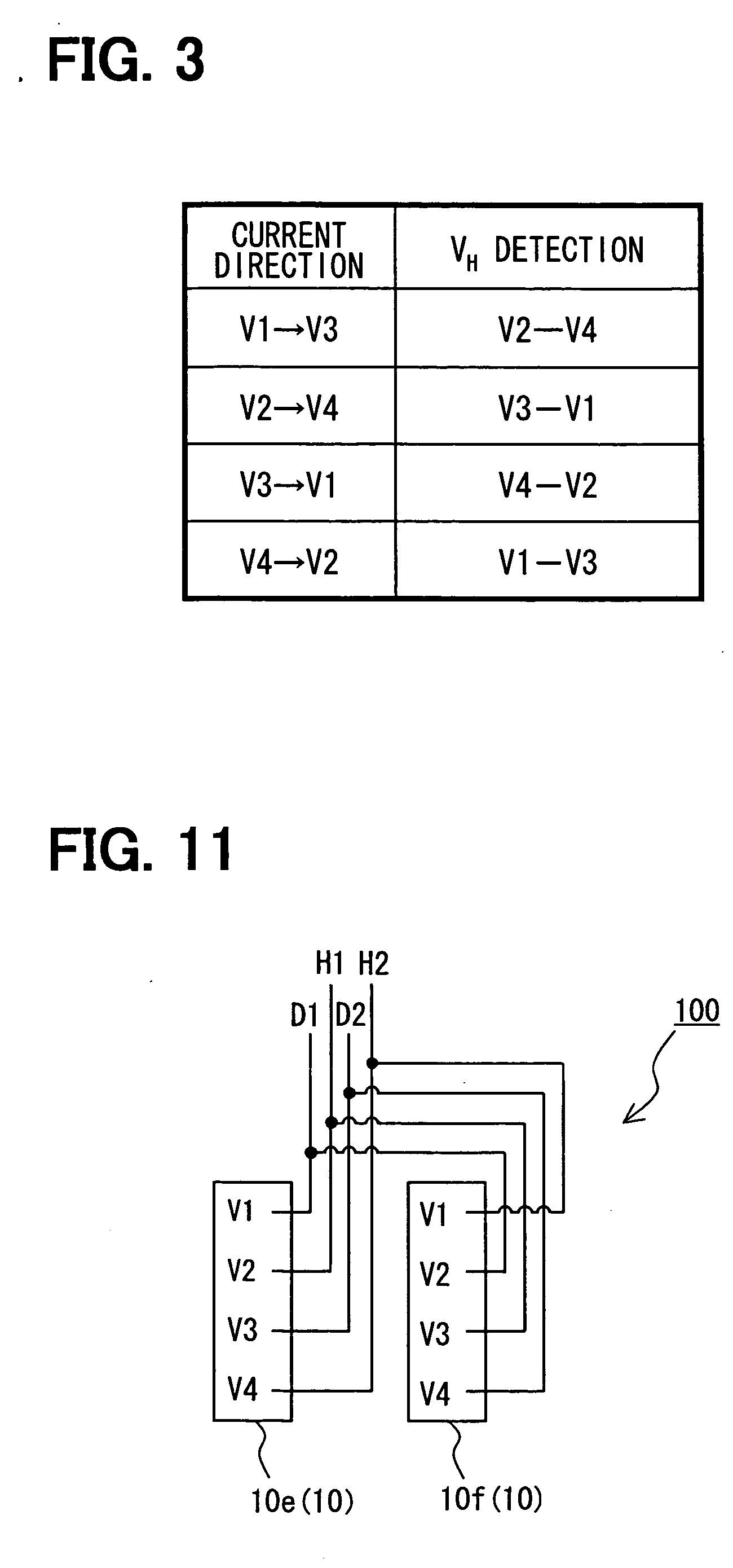
[0045]FIGS. 1A and 1B are views showing the schematic construction of a magnetic sensor in accordance with a first embodiment mode, where FIG. 1A is a plan view and FIG. 1B is a cross-sectional view along line IB-IB of FIG. 1A.

[0046] As shown in FIGS. 1A and 1B, a magnetic sensor 100 in accordance with this embodiment mode is constructed by forming a Hall element 10 of a vertical type in a substrate (semiconductor substrate) 11 constructed by a single electric conductivity type. The Hall element 10 is formed by utilizing a CMOS process. The present applicant previously discloses JP-A-2005-333103 as the magnetic sensor 100 (vertical Hall element 10) of such a construction. Accordingly, characteristic portions of this embodiment mode will next be centrally explained.

[0047] For example, the Hall element 10 of the vertical type is constructed by arranging a silicon substrate (P-sub) of P-type as a substrate 11 having a (100)-plane as a cut face, and a semiconductor area (N-well) 1...

second embodiment

Mode

[0068] A second embodiment mode will next be explained on the basis of FIGS. 5A and 5B. FIGS. 5A and 5B are views showing the schematic construction of a magnetic sensor in accordance with the second embodiment mode, where FIG. 5A is a plan view and FIG. 5B is a cross-sectional view along line VB-VB of FIG. 5A.

[0069] The magnetic sensor in accordance with the second embodiment mode is common to the magnetic sensor 100 shown in the first embodiment mode in many portions.

[0070] In the magnetic sensor 100 in accordance with this embodiment mode, the Hall element 10 of the vertical type is formed by utilizing a bipolar process. The operation and driving mode of the magnetic sensor 100 are similar to those of the first embodiment mode.

[0071] As shown in FIGS. 5A, 5B, the substrate 11 is constructed by a semiconductor substrate 11a constructed by e.g., silicon of P-type (first electric conductivity type) and a semiconductor layer 11b constructed by silicon of N-type (second electri...

third embodiment

Mode

[0081] Next, a third embodiment mode will be explained on the basis of FIGS. 7A and 7B. FIGS. 7A and 7B are views showing the schematic construction of a magnetic sensor in accordance with the third embodiment mode, where FIG. 7A is a plan view and FIG. 7B is a cross-sectional view along line VIIB-VIIB of FIG. 7A.

[0082] The magnetic sensor in accordance with the third embodiment mode is common to the magnetic sensor 100 shown in the first and second embodiment modes in many portions.

[0083] As shown in FIGS. 7A and 7B, the magnetic sensor 100 in accordance with this embodiment mode basically approximately has the same structure as the magnetic sensor 100 shown in the first embodiment mode, and its operation mode is also set as mentioned above. In this embodiment mode, an electrode material 21 of a flat plate shape constructed by e.g., aluminum, polycrystal silicon, etc. is arranged on the substrate 11 through an insulating film 20 constructed by e.g., PSG, silicon oxide, etc. i...


PUM


Abstract

A magnetic sensor includes: a substrate; a semiconductor region; a magnetic field detection portion; a pair of first electrodes; and two pairs of second electrodes. One pair of second electrodes includes first and second terminals, and the other pair includes third and fourth terminals. The first and third terminals are disposed on one side, and the second and fourth terminals are disposed on the other side. The first and fourth terminals are electrically coupled, and the second and third terminals are electrically coupled. The magnetic field detection portion and the first and second electrodes provide a vertical Hall element. One of the first and second electrodes supplies a driving current, and the other one detects the Hall voltage.

Description

CROSS REFERENCE TO RELATED APPLICATIONS [0001] This application is based on Japanese Patent Applications No. 2006-6465 filed on Jan. 13, 2006, and No. 2006-278087 filed on Oct. 11, 2006, the disclosures of which are incorporated herein by reference. FIELD OF THE INVENTION [0002] The present invention relates to a magnetic sensor and a method for detecting a magnetic field. BACKGROUND OF THE INVENTION [0003] In recent years, the magnetic sensor using the vertical Hall element for detecting a horizontal magnetic field component with respect to the surface of a substrate is proposed in, for example, “Three-dimensional integrated magnetic sensor”, Journal of IEE Japan C, pp. 483-490, No. 7, Vol. 109, 1989. FIGS. 26A and 26B are schematic constructional views showing one example of the above vertical Hall element, where FIG. 26A is a plan view, and FIG. 26B is a cross-sectional view along line XXVIB-XXVIB of FIG. 26A. [0004] As shown in FIGS. 26A and 26B, a Hall element 30 of the vertica...

Claims


Application Information

Patent Timeline
Patent Type & Authority Applications(United States)
IPC IPC(8): G01R33/06
CPCG01R33/07H01L43/065G01R33/077G01R33/075H10N52/101
Inventor OOHIRA, SATOSHIFUJII, TETSUO
Owner DENSO CORP
Why Eureka
Try Eureka