Semiconductor package having functional and auxiliary leads, and process for fabricating it
- Summary
- Abstract
- Description
- Claims
- Application Information
AI Technical Summary
Benefits of technology
Problems solved by technology
Method used
Image

Examples
Embodiment Construction
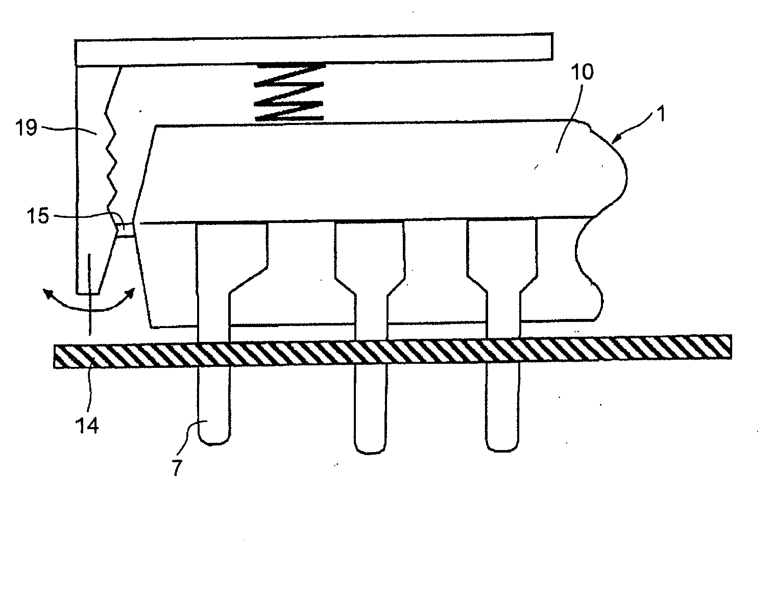
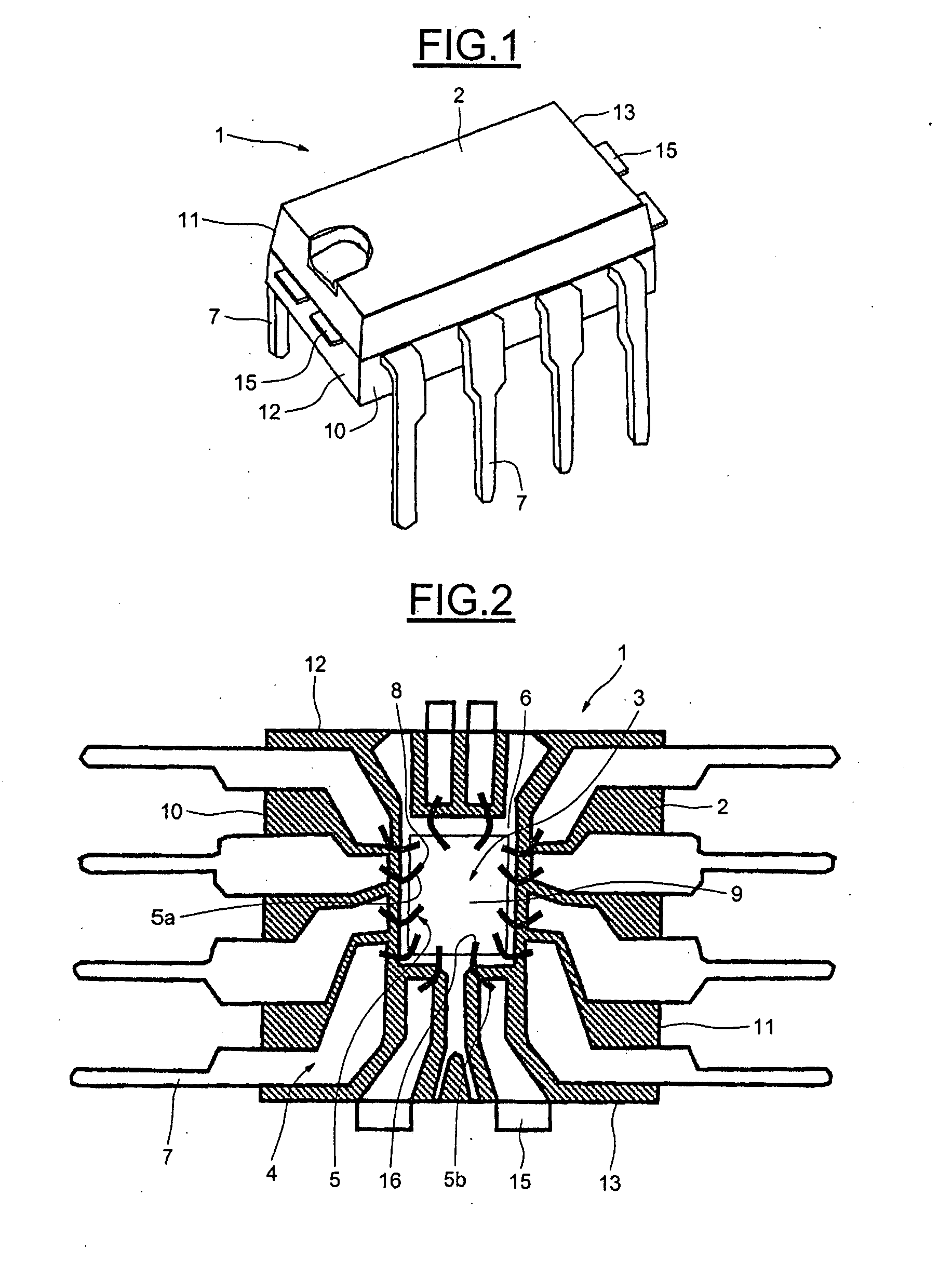
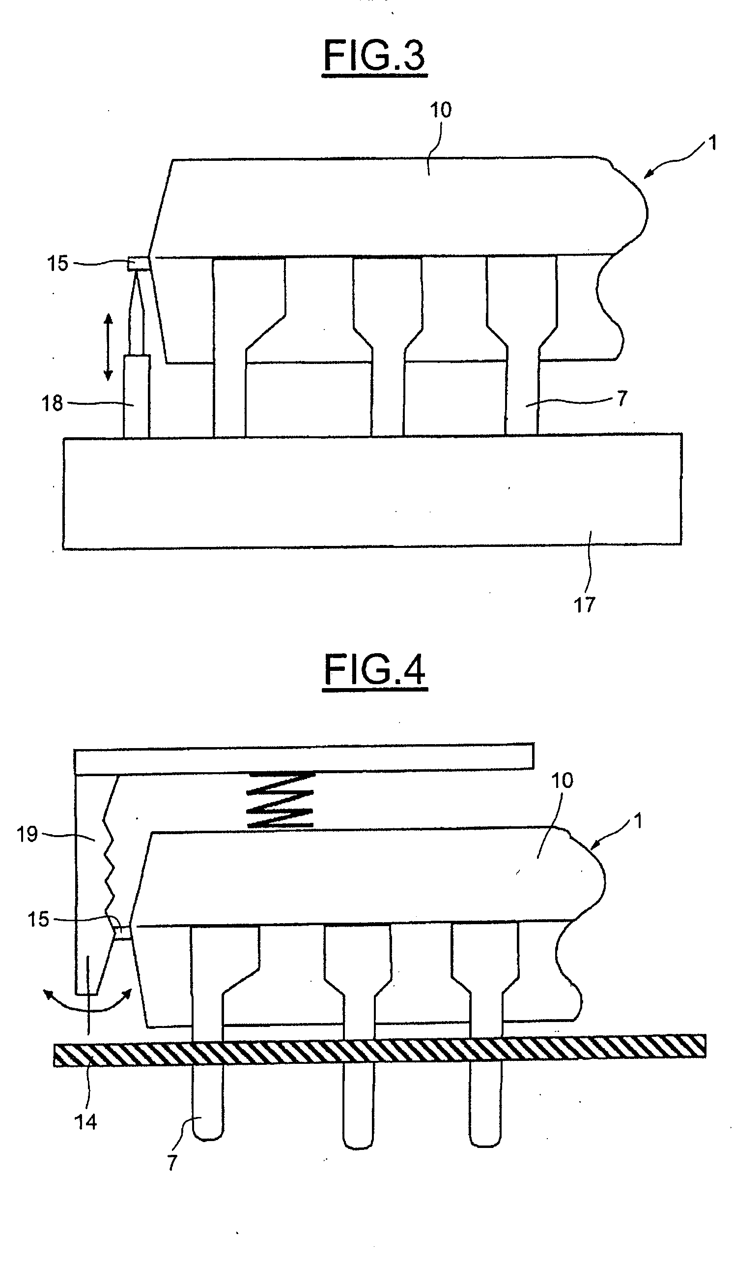
[0027] Referring in particular to FIGS. 1 and 2, it may be seen that a semiconductor package 1 comprises a substantially parallelepipedal block 2 of an encapsulation material, in which an integrated-circuit chip 3, a metal leadframe 4 and electrical connection wires 5 are embedded.
[0028] The leadframe 4 comprises a central platform 6 to which the chip 3 is bonded, a multiplicity of functional electrical connection leads 7, which extend to the periphery of the platform and emerge on the outside of the block 2, and electrical connection wires 5a selectively connecting these functional leads 7 to functional contact pads 8 on the chip 3 that are provided on a face 9 of the latter, opposite the platform 6.
[0029] In the example shown, the leadframe 4 has two sets of four functional leads 7 that emerge on the outside of the block 2 via two opposed sides 10 and 11 of this block 2.
[0030] Thus, no functional lead emerges from the block 2 via its two other opposed sides 12 and 13.
[0031] Th...
PUM
 Abstract
Description
Claims
Application Information
 - R&D Engineer
- R&D Manager
- IP Professional
- Industry Leading Data Capabilities
- Powerful AI technology
- Patent DNA Extraction
Browse by: Latest US Patents, China's latest patents, Technical Efficacy Thesaurus, Application Domain, Technology Topic.
© 2024 PatSnap. All rights reserved.Legal|Privacy policy|Modern Slavery Act Transparency Statement|Sitemap