Method of characterising the transmission losses of an optical system

a transmission loss and optical system technology, applied in the field of characterizing the transmission loss of optical systems, can solve the problems of large amount, time-consuming off-line techniques, and inability to easily detect or quantify errors in lithographic apparatuses printed in resists, and achieve the effect of reducing the effect of different transmission losses

Active Publication Date: 2007-12-27
ASML NETHERLANDS BV
View PDF36 Cites 137 Cited by
  • Summary
  • Abstract
  • Description
  • Claims
  • Application Information

AI Technical Summary

Benefits of technology

[0012]It is therefore an object of the present invention to minimise the

Problems solved by technology

Secondly, the measurements may allow errors in the lithographic apparatus, for example illumination settings or exposure dose, to be detected and correct for subsequent exposures.
However, many errors in the lithographic apparatus cannot easily be detected or quantified from the patterns printed in resist.
Such off-line techniques ta

Method used


Image

  • Method of characterising the transmission losses of an optical system
  • Method of characterising the transmission losses of an optical system
  • Method of characterising the transmission losses of an optical system

Examples


Embodiment Construction

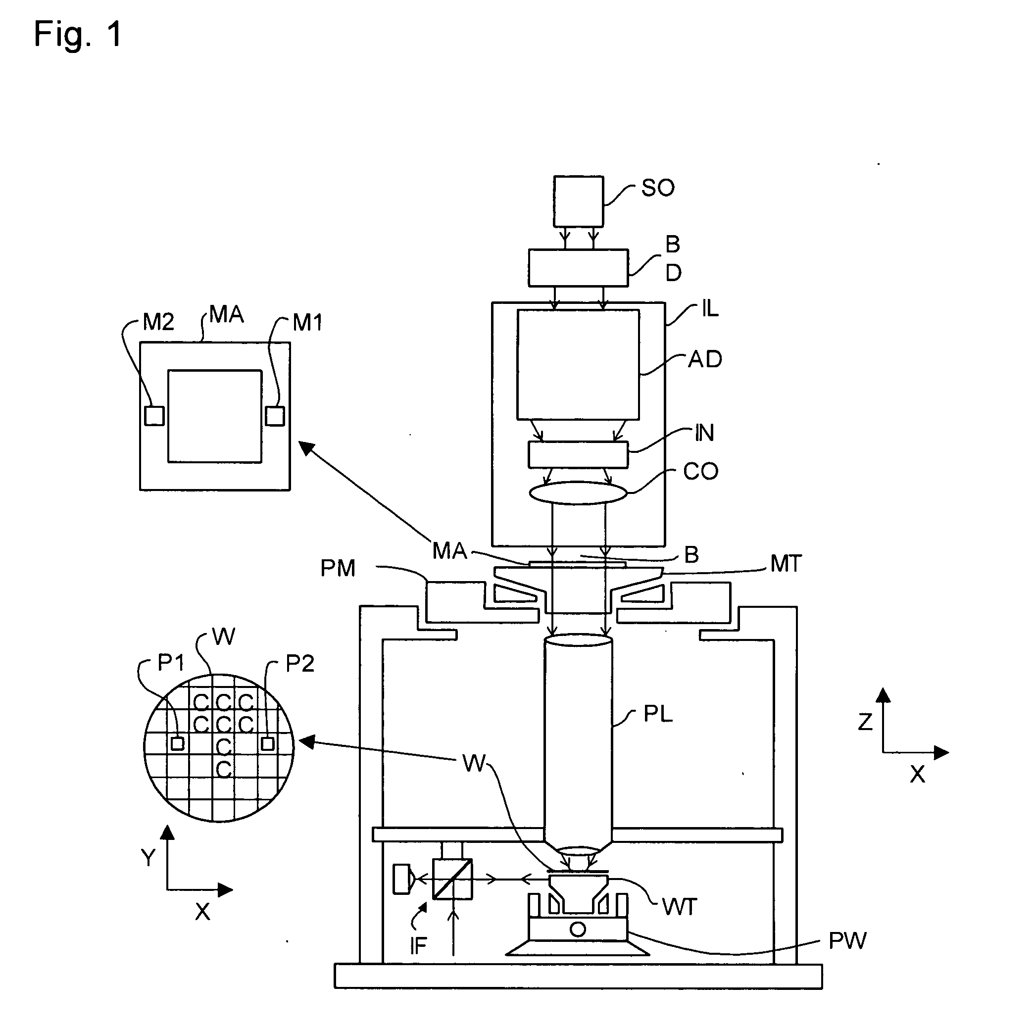
[0024]FIG. 1 schematically depicts a lithographic apparatus used in conjunction with the invention. The apparatus comprises an illumination system (illuminator) IL configured to condition a radiation beam B (e.g. UV radiation or DUV radiation). A support (e.g. a mask table) MT is configured to support a patterning device (e.g. a mask) MA and is connected to a first positioner PM configured to accurately position the patterning device in accordance with certain parameters. A substrate table (e.g. a wafer table) WT is configured to hold a substrate (e.g. a resist-coated wafer) W and is connected to a second positioner PW configured to accurately position the substrate in accordance with certain parameters. A projection system (e.g. a refractive projection lens system) PL configured to project a pattern imparted to the radiation beam B by patterning device MA onto a target portion C (e.g. comprising one or more dies) of the substrate W.

[0025]The illumination system may include various ...


PUM


Abstract

The illumination profile of a radiation beam is initially measured using a CCD detector. A reference mirror is then placed in the focal plane of the high aperture lens and the reflected radiation measured. By comparing the illumination profile and the detected radiation it is possible to determine the transmission losses for S and P polarisation which can then be used in scatterometry modeling.

Description

BACKGROUND OF THE INVENTION[0001]1. Field of the Invention[0002]The present invention relates to a method of characterizing the transmission losses of an optical system and a method of measuring properties of a substrate.[0003]2. Description of the Related Art[0004]A lithographic apparatus is a machine that applies a desired pattern onto a substrate, usually onto a target portion of the substrate. A lithographic apparatus can be used, for example, in the manufacture of integrated circuits (ICs). In that instance, a patterning device, which is alternatively referred to as a mask or a reticle, may be used to generate a circuit pattern to be formed on an individual layer of the IC. This pattern can be transferred onto a target portion (e.g. comprising part of, one, or several dies) on a substrate (e.g. a silicon wafer). Transfer of the pattern is typically via imaging onto a layer of radiation-sensitive material (resist) provided on the substrate. In general, a single substrate will co...

Claims


Application Information

Patent Timeline
IPC IPC(8): G01B9/00G01J4/00
CPCG03F7/70566G03F7/70941G03F7/70616H01L21/0274
Inventor DEN BOEF, ARIE JEFFREYCORBEIJ, WILHELMUS MARIADUSA, MIRCEAKRAAIJ, MARKUS GERARDUS MARTINUS VAN
Owner ASML NETHERLANDS BV
Why Eureka
Try Eureka