
Method for Manufacturing Heat Sink of Semiconductor Device

a technology of semiconductor devices and heat sinks, which is applied in the direction of semiconductor lasers, lasers, basic electric elements, etc., can solve the problems of poor heat sink heat sink heat sink efficiency, and achieve the effect of increasing the operation stability of the semiconductor devi

Inactive Publication Date: 2007-12-27
NAT CHENG KUNG UNIV
View PDF4 Cites 14 Cited by
  • Summary
  • Abstract
  • Description
  • Claims
  • Application Information

AI Technical Summary

Benefits of technology

[0006]In view of the above, with the exception of the flip chip technique and the thermal bonding technique, the opto-electrical device needs to be fixed to the heat sink of the opto-electrical device with glue in conventional opto-electrical device package techniques resulting in poor heat-sinking efficiency of the heat sink. Therefore, one aspect of the present invention is to provide a method for manufacturing a heat sink of a semiconductor device, which directly deposits a heat-sinking metal on a bottom surface of the semiconductor device by plating deposition, electroless plating deposition or evaporation deposition, so that the semiconductor device can adhere and be fixed to the metal heat sink without glue. As a result, the semiconductor device is closely connected with the heat-sinking metal, and the heat-sinking efficiency of the heat-sinking metal can be improved, thereby enhancing the heat-sinking ability of the semiconductor device.
[0007]Another aspect of the present invention is to provide a method for manufacturing a heat sink of an opto-electrical device, in which the metal heat sink can be directly easily deposited on a bottom surface of the opto-electrical device with adhesive tape, so that the opto-electrical device is directly and closely connected with the heat-sinking metal, thereby greatly increasing the heat-transmitting area of the opto-electrical device to enhance the heat-transmitting efficiency of the opto-electrical device.
[0008]Still another aspect of the present invention is to provide a method for manufacturing a heat sink of an opto-electrical device, which directly connects the opto-electrical device and a metal heat sink, so that the heat generated during the operation of the opto-electrical device can be transmitted rapidly, thereby rapidly lowering the temperature of the opto-electrical device, enhancing the operation quality of the opto-electrical device and prolonging the life of the opto-electrical device.
[0012]By directly forming the metal heat sink on the surface of the semiconductor device, the metal heat sink can be in direct contact with and directly connected to the semiconductor device, so that there exists no glue between the metal heat sink and the semiconductor device, thereby heat of the semiconductor device can be rapidly transmitted to the metal heat sink, the heat produced during the operation of the semiconductor device can be rapidly dissipated to further increase the operation stability of the semiconductor device.

Problems solved by technology

In view of the above, with the exception of the flip chip technique and the thermal bonding technique, the opto-electrical device needs to be fixed to the heat sink of the opto-electrical device with glue in conventional opto-electrical device package techniques resulting in poor heat-sinking efficiency of the heat sink.

Method used


Image

  • Method for Manufacturing Heat Sink of Semiconductor Device
  • Method for Manufacturing Heat Sink of Semiconductor Device
  • Method for Manufacturing Heat Sink of Semiconductor Device

Examples


Embodiment Construction

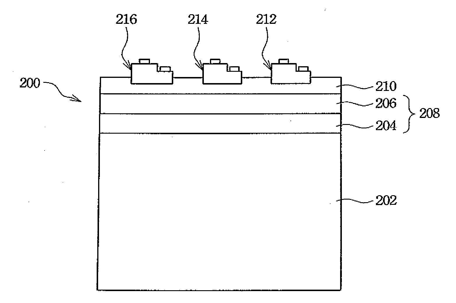
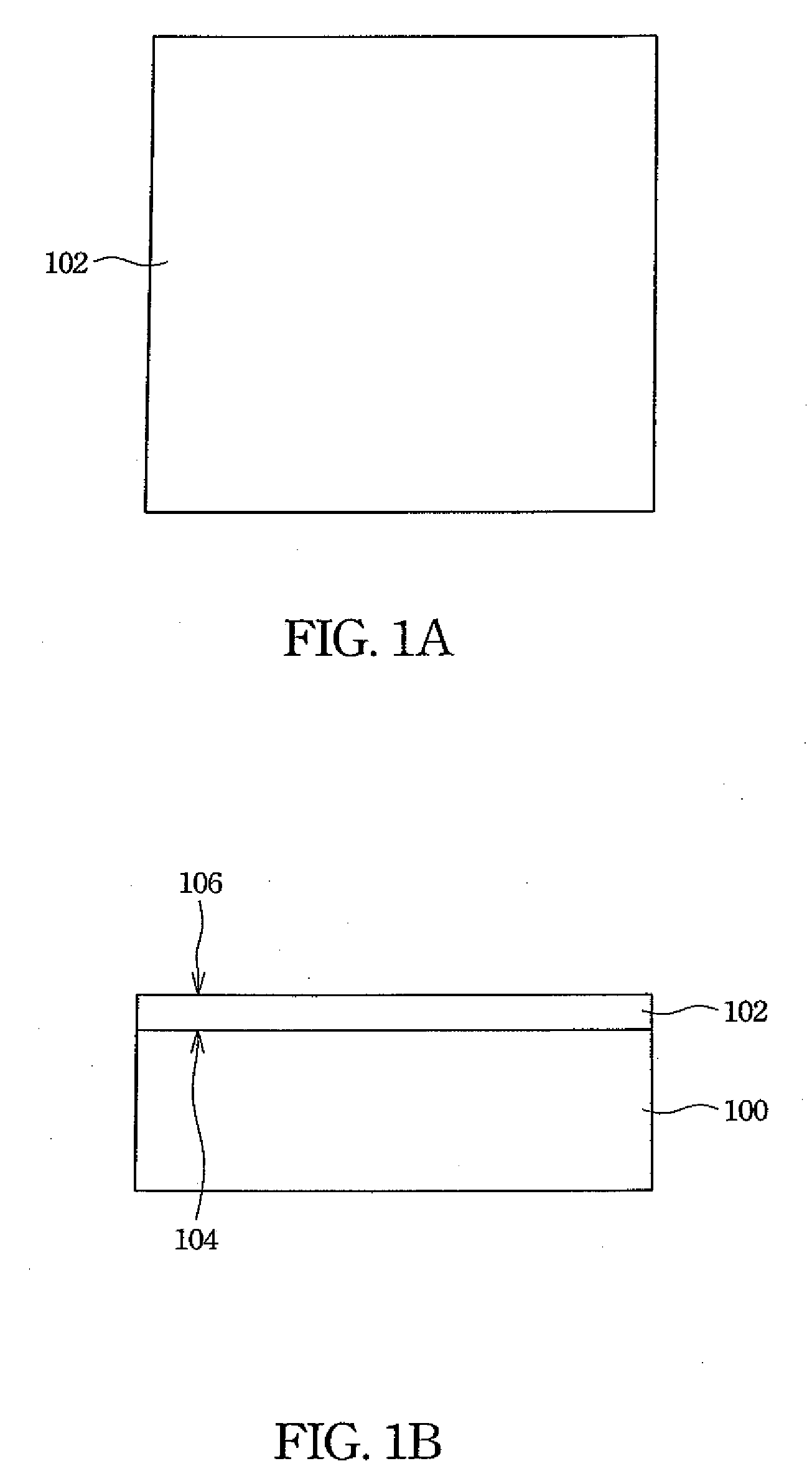
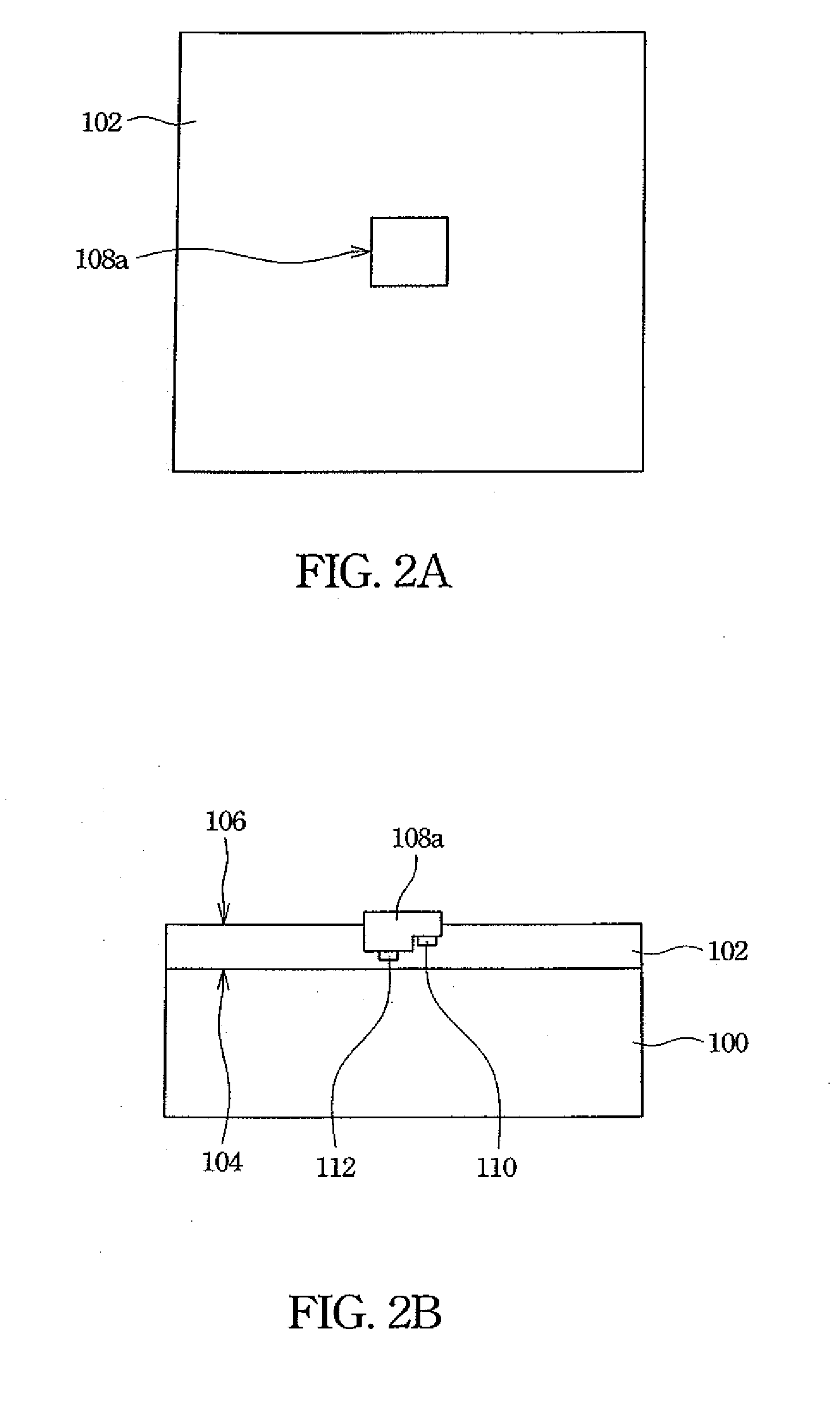
[0016]The present invention discloses a method for manufacturing a heat sink of a semiconductor device, which can make the heat sink directly adhere to and contact with the semiconductor device, thereby greatly enhancing the heat-sinking efficiency of the heat sink and effectively prolonging the life of the semiconductor device. In order to make the illustration of the present invention more explicit, the following description is stated with reference to FIG. 1A to FIG. 7.

[0017]FIG. 1A to FIG. 6 are schematic flow diagrams showing the process for manufacturing a semiconductor device in accordance with a preferred embodiment of the present invention, wherein the schematic flow diagrams includes cross-sectional views and the corresponding top views. Firstly, a temporary substrate 100 and an adhesive tape 102 are provided, wherein the adhesive tape 102 includes surfaces 104 and 106 on opposite sides. The surface 104 of the adhesive tape 102 adheres directly to a surface of the temporar...


PUM


Abstract

A method for manufacturing a heat sink of a semiconductor device is described. In the method, an adhesive tape is provided, wherein the adhesive tape includes a first surface and a second surface on opposite sides, and the first surface of the adhesive tape adheres to a surface of a temporary substrate. At least one semiconductor device is provided, wherein the semiconductor device includes a first side and a second side opposite to the first side, and the first side of the one semiconductor device is pressed and set into a portion of the second surface of the adhesive tape, and the second side of the one semiconductor device is exposed. A thin metal layer is formed on the second side of the semiconductor device and the exposed portion of the second surface of the adhesive tape. A metal heat sink is formed on the thin metal layer. Then, the adhesive tape and the temporary substrate are removed.

Description

RELATED APPLICATIONS[0001]The present application is based on, and claims priority from, Taiwan Application Serial Number 95123021, filed Jun. 26, 2006, the disclosure of which is hereby incorporated by reference herein in its entirety.FIELD OF THE INVENTION[0002]The present invention relates to a method for manufacturing a heat sink of a semiconductor device, and more particularly, to a method for manufacturing a heat sink of an opto-electrical device.BACKGROUND OF THE INVENTION[0003]When small solid state opto-electrical devices, such as light-emitting diodes (LEDs) or laser diodes (LDs), are applied in a large or small backlight module or illumination module, a lot of opto-electrical devices are needed for the requirements of brightness or illumination of these modules. However, when the opto-electrical devices are operated at high power, the temperature of the module composed of the opto-electrical devices rapidly increases, degrading the operation quality of the module and ulti...

Claims


Application Information

Patent Timeline
IPC IPC(8): H01L21/00H01L23/36
CPCH01L33/0079H01L33/641H01S5/02256H01S5/4093H01S5/024H01S5/02476H01S5/02272H01L33/0093H01S5/02355H01S5/0237H01L23/36
Inventor SU, YAN-KUINCHEN, KUAN-CHUNLIN, CHUN-LIANGHUANG, JIN-QUANHU, SHU-KAI
Owner NAT CHENG KUNG UNIV
Learn More