

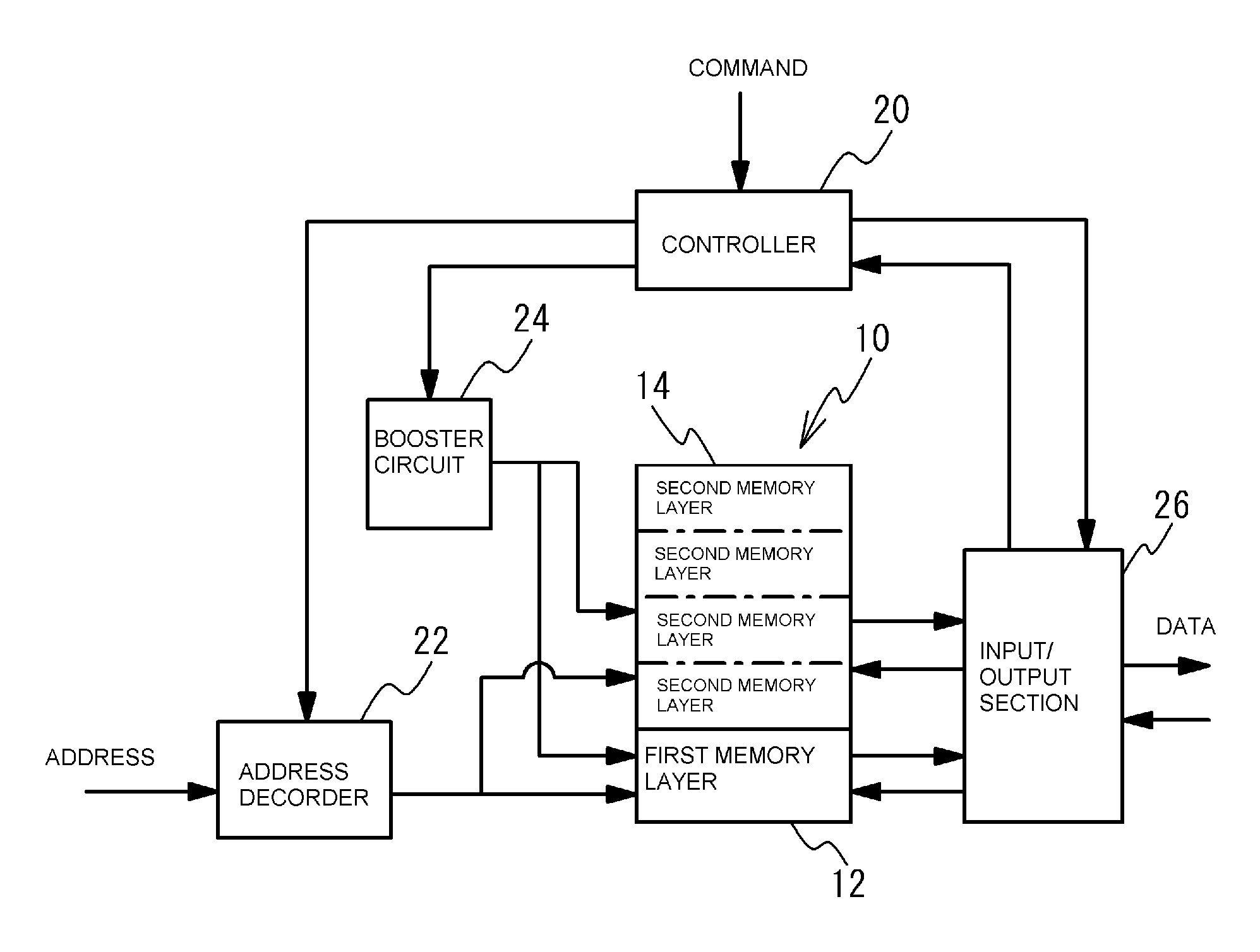
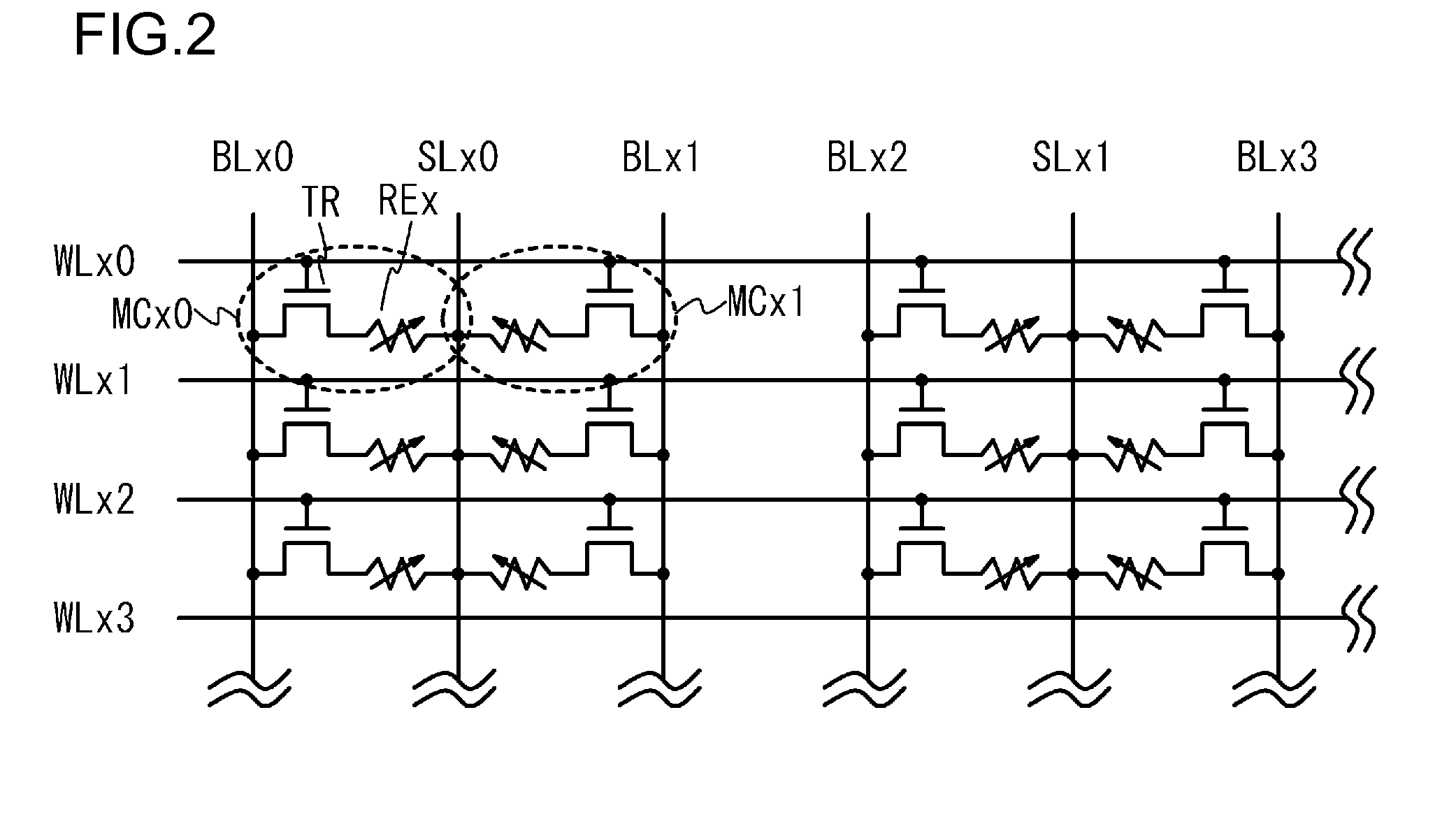
Semiconductor memory device with stacked memory cell structure
a memory cell and semiconductor technology, applied in semiconductor devices, digital storage, instruments, etc., can solve the problems of unreliable, difficult voltage control, and difficult integration of memory elements, and achieve excellent reliability of holding data, high operation reliability, and improved operation stability of semiconductor devices
- Summary
- Abstract
- Description
- Claims
- Application Information
AI Technical Summary
Benefits of technology
Problems solved by technology
Method used
Image

Examples
Embodiment Construction
[0034]Reference will now be made in detail to the preferred embodiments of the claimed subject matter, a method and system for the use of a reputation service provider, examples of which are illustrated in the accompanying drawings. While the claimed subject matter will be described in conjunction with the preferred embodiments, it will be understood that they are not intended to be limit to these embodiments. On the contrary, the claimed subject matter is intended to cover alternatives, modifications and equivalents, which may be included within the spirit and scope as defined by the appended claims.
[0035]Furthermore, in the following detailed descriptions of embodiments of the claimed subject matter, numerous specific details are set forth in order to provide a thorough understanding of the claimed subject matter. However, it will be recognized by one of ordinary skill in the art that the claimed subject matter may be practiced without these specific details. In other instances, w...
PUM
 Abstract
Description
Claims
Application Information