

Substrate bonding method
- Summary
- Abstract
- Description
- Claims
- Application Information
AI Technical Summary
Benefits of technology
Problems solved by technology
Method used
Image

Examples
Embodiment Construction
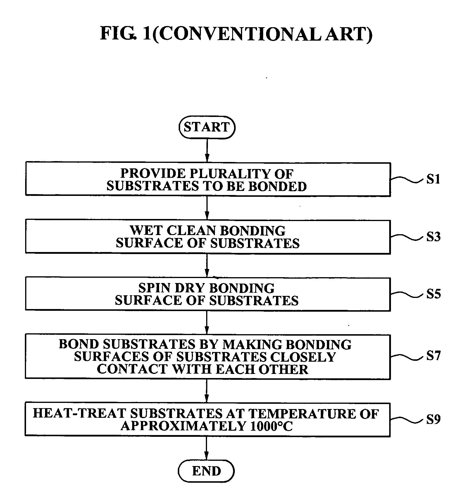
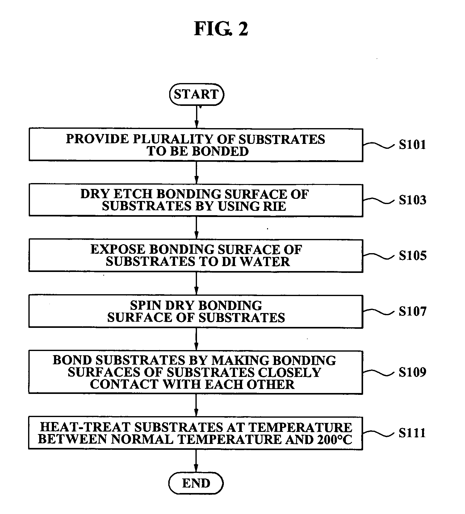
[0030]Referring to FIGS. 2 and 3A through 3D, the substrate bonding method according to an exemplary embodiment of the present invention is described.
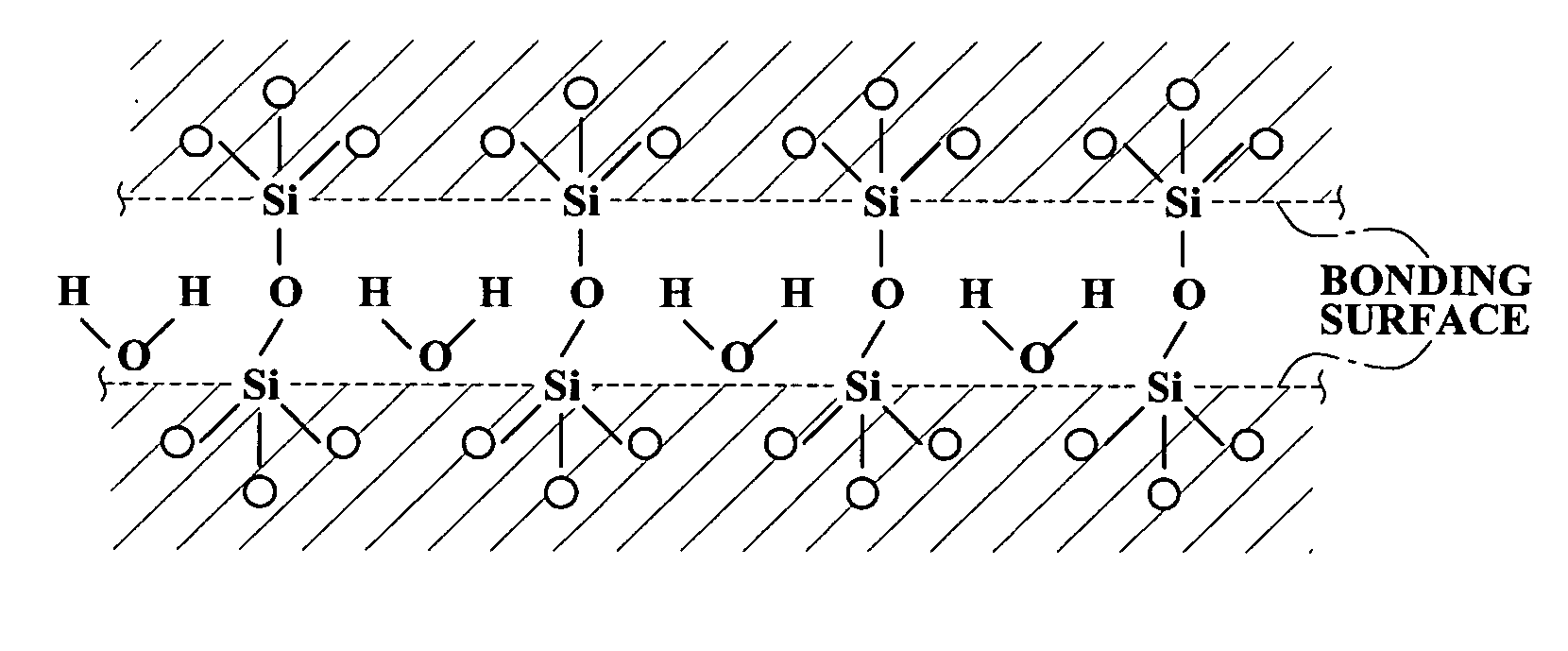
[0031]FIG. 2 is a flowchart illustrating a substrate bonding method according to an exemplary embodiment of the present invention. FIGS. 3A through 3D are chemical structures sequentially illustrating a bonding configuration of substrates in a substrate bonding method according to an exemplary embodiment of the present invention.
[0032]In step S101, a plurality of substrates to be bonded is provided. In one embodiment, the substrates are silicon wafers.
[0033]While a method of bonding two substrates each having a respective bonding surface will be described in detail as an example below, it should be noted that the same process may apply to the cases where three substrates or more are bonded together.
[0034]In step S103, the bonding surface of the substrates is dry etched. Etching is generally used to create a pattern on a substrate. In t...
PUM
 Abstract
Description
Claims
Application Information