
Top-emitting N-based light emitting device and method of manufacturing the same

a technology of light emitting devices and n-based ohmic contacts, which is applied in the direction of semiconductor/solid-state device manufacturing, semiconductor/ni/au ohmic contact layer not suitable for large-capacity and high-brightness light emitting devices, etc., to achieve the effect of increasing the light extraction ra

Active Publication Date: 2008-01-10
KOREA UNIV RES & BUSINESS FOUND +1
View PDF9 Cites 27 Cited by
  • Summary
  • Abstract
  • Description
  • Claims
  • Application Information

AI Technical Summary

Benefits of technology

[0010]Example embodiments provide an N-based light emitting device including an electrode structure having an increased light extraction rate by inducing a diffused reflection of light generated in the light emitti

Problems solved by technology

However, even though much research on light emitting devices using N-based compound semiconductors has been recently conducted, a high quality ohmic contact cannot easily be obtained because a p-GaN has low carrier concentration, high sheet resistance, and low electrical conductivity.
However, the conventional Ni / Au ohmic contact layer is not suitable for use in large capacity and high brightness light emitting devices due to the low light extraction rate by having a low light transmittance of about 75% when the thickness of the layer is 450 nm.
However, electrode-surface texturing and patterning require additional processes involving a mask and dry-etching.
Thus, these methods are not effective for manufacturing light emitting devices.
The electrode-surface may be damaged by the dry-etching process in the manufacturing of the N-based light emitting devices.
Further, the light extraction rate of light emitting devices that emit light having a wavelength in the range of 400 to 500 nm cannot be maximized because the light emitting devices manufactured by these electrode-surface texturing and patterning methods have micro-meter sized hole patterns.

Method used


Image

  • Top-emitting N-based light emitting device and method of manufacturing the same
  • Top-emitting N-based light emitting device and method of manufacturing the same
  • Top-emitting N-based light emitting device and method of manufacturing the same

Examples


Embodiment Construction

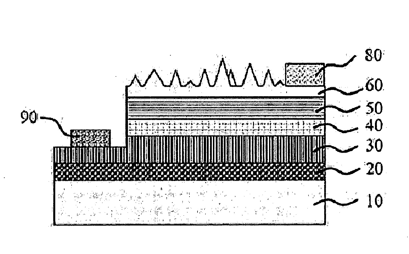
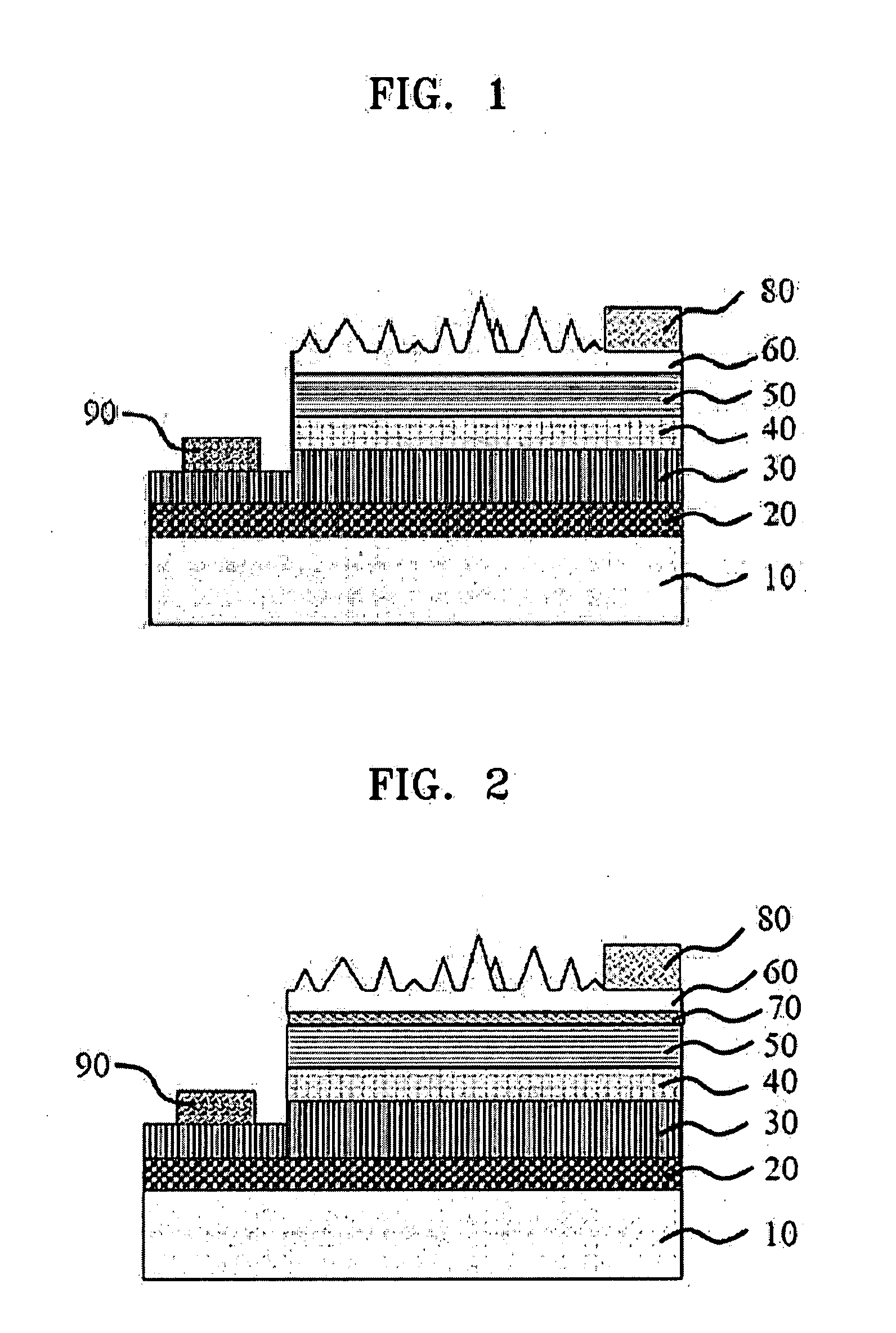
[0030]Reference will now be made in detail to example embodiments, examples of which are illustrated in the accompanying drawings. However, example embodiments are not limited to the embodiments illustrated hereinafter, and the embodiments herein are rather introduced to provide easy and complete understanding of the scope and spirit of example embodiments. In the drawings, the thicknesses of layers and regions are exaggerated for clarity.

[0031]It will be understood that when an element or layer is referred to as being “on,”“connected to” or “coupled to” another element or layer, it may be directly on, connected or coupled to the other element or layer or intervening elements or layers may be present. In contrast, when an element is referred to as being “directly on,”“directly connected to” or “directly coupled to” another element or layer, there are no intervening elements or layers present. Like reference numerals refer to like elements throughout. As used herein, the term “and / or...


PUM


Abstract

Provided is a top-emitting N-based light emitting device and a method of manufacturing the same. The N-based light emitting device may include an n-type clad layer, an active layer, a p-type clad layer, and a transparent conductive thin film which may be sequentially stacked on a substrate. The transparent conductive thin film may have a surface nano-scale patterned by wet-etching and then annealing without using a mask for improving the light extraction rate. A light emitting device having a higher brightness may be prepared by increasing or maximizing the light extraction rate by employing the transparent conductive thin film having the surface patterned by wet-etching and then annealing.

Description

PRIORITY STATEMENT[0001]This application claims priority under 35 USC §119 to Korean Patent Application No. 2006-0056373, filed on Jun. 22, 2006, in the Korean Intellectual Property Office (KIPO), the entire contents of which are herein incorporated by reference.BACKGROUND[0002]1. Field[0003]Example embodiments relate to a top-emitting N-based light emitting device with an increased light extraction rate including a nano-scale patterned transparent conductive thin film that is prepared by wet-etching and annealing the surface of the transparent conductive thin film without using a mask, and a method of manufacturing the same.[0004]2. Description of Related Art[0005]When a light emitting device is formed using an N-based compound semiconductor (e.g., GaN-based compound semiconductor), a process of forming a high quality ohmic contact between the semiconductor and the electrode is required. However, even though much research on light emitting devices using N-based compound semiconduct...

Claims


Application Information

Patent Timeline
IPC IPC(8): H01L33/00H01L33/06H01L33/12H01L33/32H01L33/38H01L33/42
CPCH01L33/42H01L33/22
Inventor SEONG, TAE-YEONLEE, TAK-HEELEEM, DONG-SEOK
Owner KOREA UNIV RES & BUSINESS FOUND
Features
  • Generate Ideas
  • Intellectual Property
  • Life Sciences
  • Materials
  • Tech Scout
  • Unparalleled Data Quality
  • Higher Quality Content
  • 60% Fewer Hallucinations
Learn More