Active devices array substrate and repairing method thereof
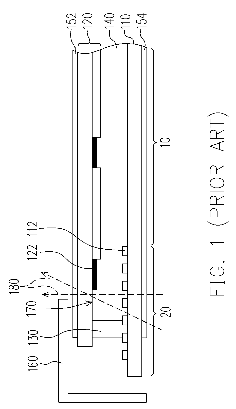
a technology of active devices and array substrates, which is applied in the direction of radiofrequency controlled devices, optics, instruments, etc., can solve the problems of unsuitable for fabricating large-scale lcd panels and slow process
- Summary
- Abstract
- Description
- Claims
- Application Information
AI Technical Summary
Benefits of technology
Problems solved by technology
Method used
Image
Examples
first embodiment
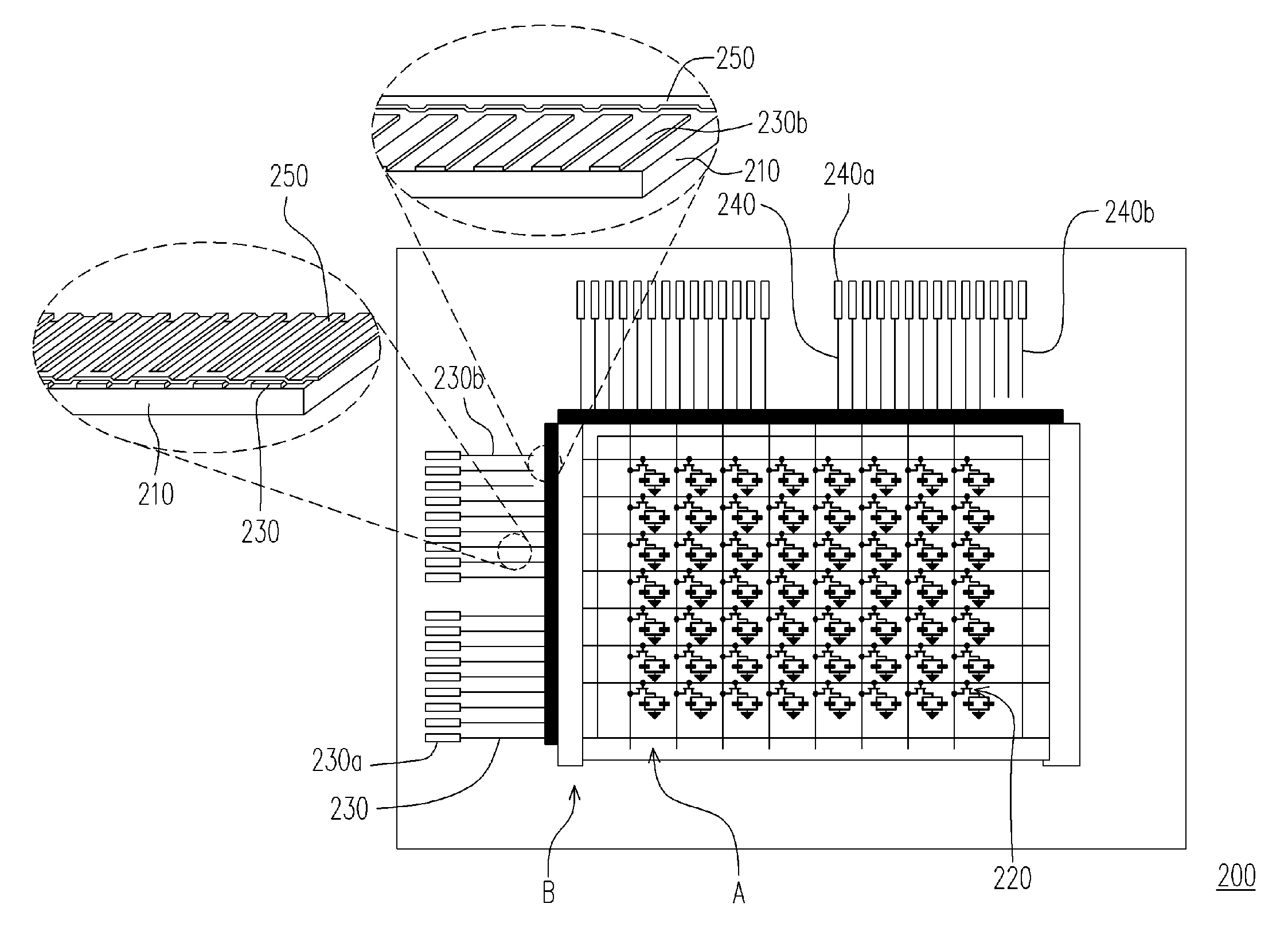
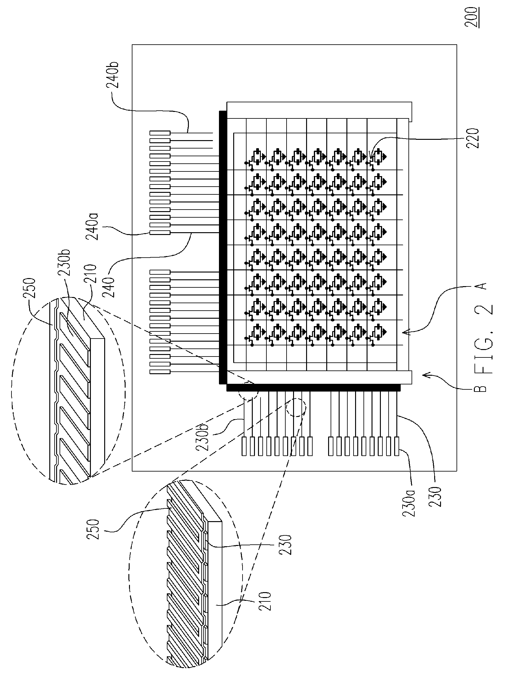
[0043]FIG. 2 is a schematic showing an active devices array substrate of the present invention. FIG. 3 is a schematically partial cross-sectional view showing an active devices array substrate according to one embodiment of the present invention. Referring to FIG. 2 and FIG. 3, the active devices array substrate 200 of the present invention includes a substrate 210, a plurality of active devices 220, a plurality of first lead lines 230, a plurality of second lead lines 240 and a first floating light-shielding layer 250. The substrate 210 has a display region A and a peripheral circuit region B surrounding display region A. The active devices 220 are arranged within the display region A on the substrate 210. Wherein, the active device 220 is, for example, a thin film transistor (TFT). Each of the active devices 220 includes a first conductive layer 220a (as shown in FIG. 3) and a second conductive layer 220b. For convenient illustrating, each of the first conductive layers 220a is c...
second embodiment
[0049]FIG. 7 is a schematic diagram showing the active devices array substrate according to the present invention. Referring to FIG. 7, the active devices array substrate 200 further comprises a ESD protection circuit 260 disposed between the display region A and the first floating light-shielding layer 250 and electrically connected with the first floating light-shielding layer 250. Thus, the electrostatic charges on the first floating light-shielding layer 250 can be dissipated by the ESD protection circuit 260 to avoid the ESD damage caused between the first floating light-shielding layer 250 and the first lead lines 230.
[0050]The ESD protection circuit 260 may be the inner guard rings used in the conventional LCD for eliminating the electrostatic charges within the display region. More detailed, the ESD protection circuit 260, for example, comprises a plurality of protection rings 262 (only one of them is shown in FIG. 7 for illustrating) and a connecting wire 264. Wherein, the ...
third embodiment
[0053]FIG. 8 is a schematic diagram showing the active devices array substrate according to the present invention. Referring to FIG. 8, the ESD protection circuit 270 of this embodiment is electrically connected with the first pads 230a, and the first floating light-shielding layer 250 is disposed between the ESD protection circuit 270 and the display region A. Particularly, the active devices array substrate 200 of this embodiment further comprises a plurality of first electrostatic guiding devices 280 disposed between the ESD protection circuit 270 and the first floating light-shielding layer 250. Each of the first electrostatic guiding devices 280 is electrically connected with the corresponding first pad 230a and the first floating light-shielding layer 250.
[0054]In more detail, each first electrostatic guiding device 280, for example, is a transistor in this embodiment. A gate 280g and a drain 280d of the transistor are electrically connected with the corresponding first pad 23...
PUM
 Abstract
Description
Claims
Application Information


