Bottom substrate of package on package and manufacturing method thereof

a technology of packaging and bottom substrate, which is applied in the direction of semiconductor devices, semiconductor/solid-state device details, electrical devices, etc., can solve the problems of increasing the total thickness of the package, reaching the limit of realizing a pop, and unable to increase the number of ics mounted on the bottom substrate, etc., to achieve the effect of increasing the overall thickness

Inactive Publication Date: 2008-01-10
SAMSUNG ELECTRO MECHANICS CO LTD
View PDF3 Cites 152 Cited by
  • Summary
  • Abstract
  • Description
  • Claims
  • Application Information

AI Technical Summary

Benefits of technology

[0012]Aspects of the present invention provide a bottom substrate of a package on package and manufacturing method thereof that ensures the gap between packages such that two or more electronic devices can be mounted on a bottom substrate without increasing the overall thickness, to implement a POP.

Problems solved by technology

However, this approach reached a limit in realizing a POP, because the total thickness of a package increased in the case of mounting two or more ICs on a substrate.
As described in the above, there is a demand for the multi-stack, in which two or more ICs are mounted, but it is difficult to increase the number of ICs mounted on a bottom substrate while maintaining the overall height of a POP by conventional manufacturing methods.
However, with the occurrence of the function-error generated when operating for a long period of time the IC chip to which the method has been applied, attempts have been made to rather reduce the substrate thickness so as to raise the mount capability of POP and implement the multi stack.
Also, in the conventional POP, in the case of manufacturing an IC thinner, in order to stack two or more ICs on a bottom substrate, problems in handling, and warpage, etc. are caused.
However, as the number of ICs stacked is increased, increasing the number of solder balls poses limits in designing the number of and intervals between solder ball pads.

Method used


Image

  • Bottom substrate of package on package and manufacturing method thereof
  • Bottom substrate of package on package and manufacturing method thereof
  • Bottom substrate of package on package and manufacturing method thereof

Examples


Embodiment Construction

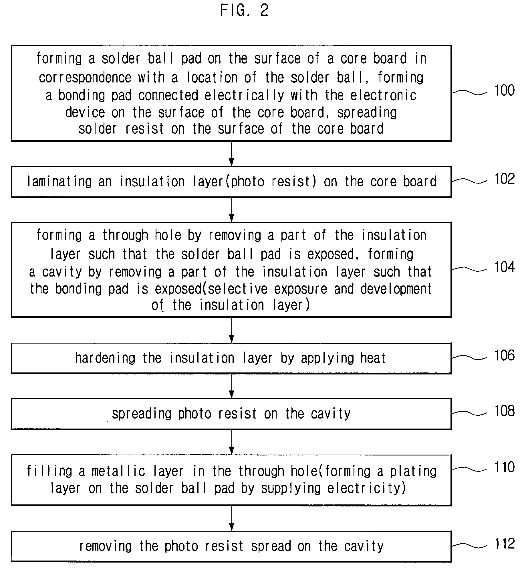
[0033]Certain embodiments of the present invention will be described below in more detail with reference to the accompanying drawings. In the description with reference to the accompanying drawings, those components are rendered the same reference number that are the same or are in correspondence regardless of the figure number, and redundant explanations are omitted.

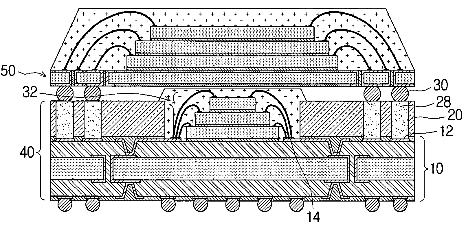
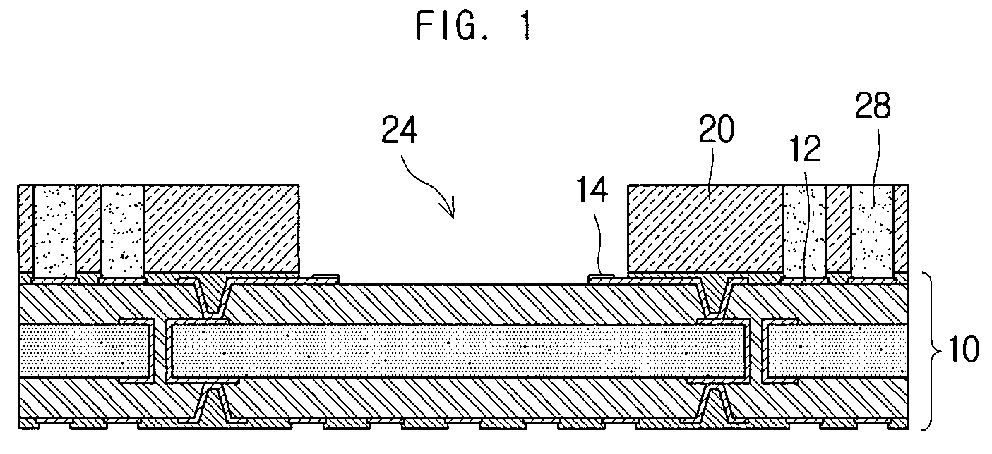
[0034]FIG. 1 is a cross-sectional view illustrating an embodiment of a bottom substrate of package on package according to the present invention. Referring to FIG. 1, a core board 10, solder ball pads 12, bonding pads 14, an insulation layer 20, a cavity 24, and a metallic layer 28 are illustrated.

[0035]The present embodiment is characterized by manufacturing the core board 10 of a bottom substrate having a layer or multi-layers of a circuit pattern formed by a conventional method of manufacturing a printed circuit board, and then ensuring the gap between packages by interposing the insulation layer 20 formed by hardeni...


PUM


Abstract

A bottom substrate of package on package and manufacturing method thereof is disclosed. A bottom substrate of a package on package electrically connected to a top substrate by means of a solder ball, including a core board, a solder ball pad formed on a surface of the core board in correspondence with a location of the solder ball, an insulation layer laminated on the core board, a through hole formed by removing a part of the insulation layer such that the solder ball pad is exposed, and a metallic layer filled in the through hole and connected electrically with the solder ball, allows the number of ICs mounted on a bottom substrate to be increased without increasing the size of a solder ball, and allows the size and pitch of the solder balls to be made smaller by controlling the thickness of the insulation layer laminated on the bottom substrate, whereby more signal transmission is possible between a top substrate and a bottom substrate.

Description

CROSS-REFERENCE TO RELATED APPLICATIONS[0001]This application claims the benefit of Korean Patent Application No. 10-2006-0063633 filed with the Korean Intellectual Property Office on Jul. 6, 2006, the disclosure of which is incorporated herein by reference in its entirety.BACKGROUND[0002]1. Technical Field[0003]The present invention relates to a bottom substrate of a package on package and a manufacturing method thereof.[0004]2. Description of the Related Art[0005]With developments in the electronics industry, there are requests for high performance, high density and miniaturization for electronic components. In order to meet these requests, there is a growing number of proposals and demands for realizing the so called ‘package substrate’ manufactured by mounting electronic devices such as ICs on printed circuit boards, where the so called ‘package on package (POP)’ manufactured by laminating another package substrate on a package substrate is gaining attention as a good alternativ...

Claims


Application Information

Patent Timeline
Patent Type & Authority Applications(United States)
IPC IPC(8): H01L23/52H01L21/00
CPCH01L25/105H01L2225/1058H01L2224/32225H01L2224/48091H01L2224/48225H01L2224/48227H01L2224/73265H01L2225/0651H01L2225/06541H01L2225/06568H01L2225/06586H01L2924/01078H01L2924/15311H01L2924/15331H01L2224/32145H01L2924/3511H01L2924/01087H01L24/48H01L25/0657H01L23/3128H01L2924/00014H01L2924/00H01L2924/00012H01L24/73H01L2924/14H01L2924/181H01L2224/45099H01L2224/45015H01L2924/207H01L23/12
Inventor PARK, JUNG-HYUNMIN, BYOUNG-YOULYOO, JE-GWANGKANG, MYUNG-SAMJUNG, HOE-KUKIM, JI-EUN
Owner SAMSUNG ELECTRO MECHANICS CO LTD
Why Eureka
Try Eureka