Semiconductor device including A/D converter

a technology of a/d converter and a/d converter, which is applied in the direction of code conversion, transmission system, instruments, etc., can solve the problems of increasing the time required to perform operations on the a/d conversion results, increasing test costs, and enormous amounts of digital output, so as to reduce the volume of data and facilitate the effect of performing

Inactive Publication Date: 2008-01-10
SOCIONEXT INC
View PDF2 Cites 8 Cited by
  • Summary
  • Abstract
  • Description
  • Claims
  • Application Information

AI Technical Summary

Benefits of technology

[0010]According to the present invention, the influence of power supply voltage variation and of noise occurring when A/D conversion results are output is avoided to easily perform an appropriate test on the A/D converter, while operation processing on the massive amounts of digital output results that are required for the test on the A/D converter due to the inc

Problems solved by technology

Nevertheless, since the number of bits of the resolution of recently fabricated A/D converters has been increasing (equal to or higher than 12 to 14 bits), enormous amounts of digital output results are necessary to test the A/D converter.
In the case where the conventional storage means is provided for the tempora

Method used


Image

  • Semiconductor device including A/D converter
  • Semiconductor device including A/D converter
  • Semiconductor device including A/D converter

Examples


first embodiment

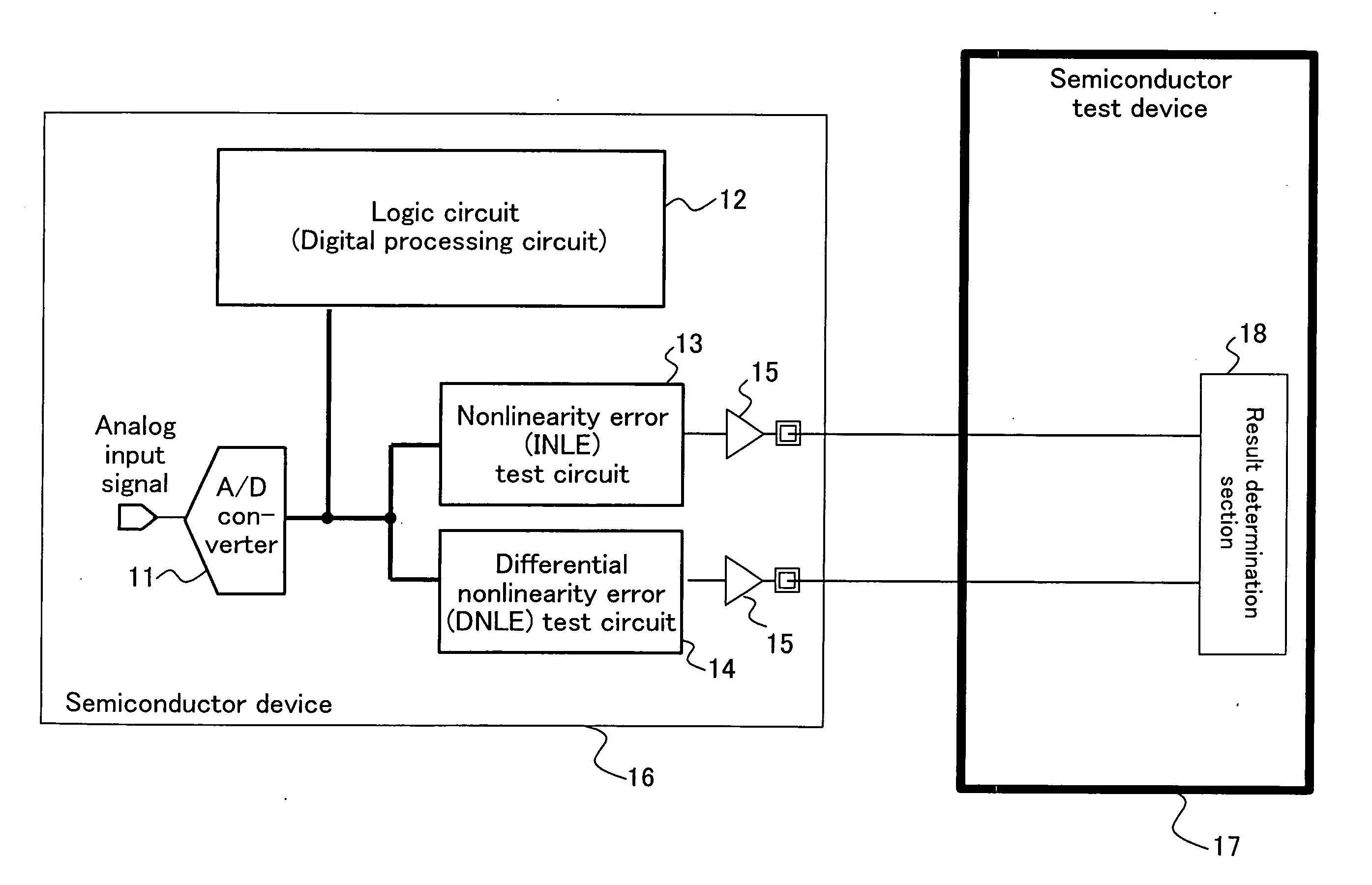
[0034]FIG. 1 illustrates the structure of a semiconductor device according to a first embodiment. The semiconductor device 16 includes an A / D converter 11, a digital processing circuit 12, a nonlinearity error (INLE) test circuit 13, a differential nonlinearity error (DNLE) test circuit 14, and buffers 15. The A / D converter 11 converts an analog input signal, which is input within or outside from the semiconductor device 16, to a digital signal. The digital processing circuit 12 performs certain processing by using conversion results obtained by the A / D converter 11 (in FIG. 1, only one bit of the output of the A / D converter 11 is described as a representative example). The nonlinearity error (INLE) test circuit 13 receives the conversion results obtained by the A / D converter 11, performs an operation for calculating a nonlinearity error (INLE) value, and outputs the operation result to a result determination section 18 in a semiconductor test device 17. The differential nonlinearit...

second embodiment

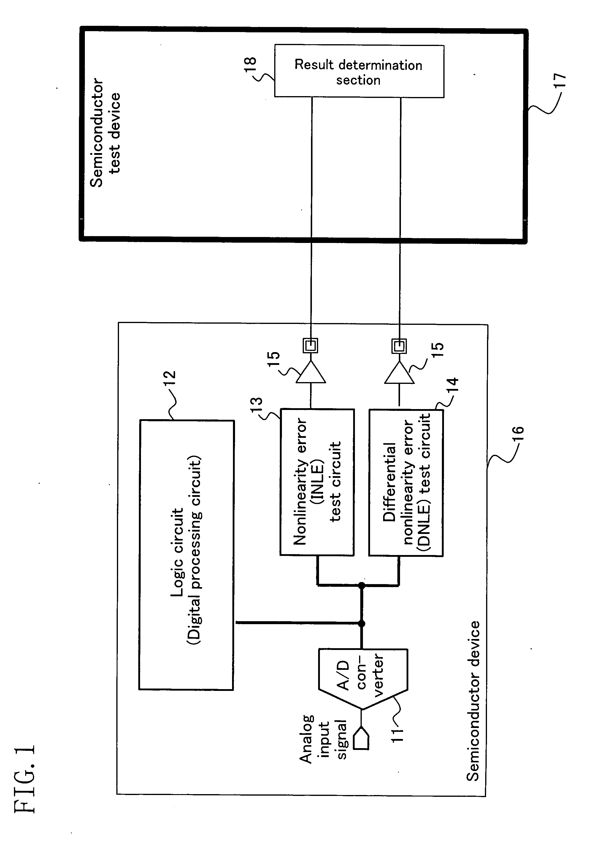
[0045]As shown in FIG. 2, a semiconductor device according to a second embodiment includes an A / D converter 11, a digital processing circuit 12, a nonlinearity error (INLE) test pre-processing and operation circuit 21, a differential nonlinearity error (DNLE) test pre-processing and operation circuit 22, and buffers 15. The A / D converter 11 and the digital processing circuit 12 are the same as those in the first embodiment.

[0046]The nonlinearity error (INLE) test pre-processing and operation circuit 21 receives conversion results obtained by the A / D converter 11, performs part of an operation for calculating a nonlinearity error (INLE) value, and outputs the operation result to a nonlinearity error (INLE) test post-processing and operation circuit 19 in a semiconductor test device 17. The differential nonlinearity error (DNLE) test pre-processing and operation circuit 22 receives the conversion results obtained by the A / D converter 11, performs part of an operation for calculating a...

third embodiment

[0053]As shown in FIG. 3, a semiconductor device according to a third embodiment includes an A / D converter 11, a digital processing circuit 12, an occurrence frequency counter circuit 25, a selector 27, and a buffer 15. The A / D converter 11 and the digital processing circuit 12 are the same as those in the first embodiment. The occurrence frequency counter circuit 25 includes an occurrence frequency sorting circuit 23, a storage circuit 24, and a read circuit 26.

[0054]Occurrence frequencies (histogram) for conversion results obtained by the A / D converter 11, i.e., for the respective output codes of A / D conversions, are stored in the occurrence frequency counter circuit 25. After the completion of a predetermined test process for the A / D converter 11 (for example, in the case of an A / D converter with a resolution of 12 bits, each time an analog input signal, a triangular wave, is input, 20,000 data pieces are captured at regular time intervals, and this is repeated ten times), the oc...


PUM


Abstract

A semiconductor device includes: an A/D converter; a digital processing circuit for performing processing based on conversion results from the A/D converter; a first test circuit for performing operation processing for checking a nonlinearity error (INLE) of the conversion results from the A/D converter; and a second test circuit for performing operation processing for checking a differential nonlinearity error (DNLE) of the conversion results from the A/D converter. The first test circuit performs only part of the operation processing for checking the nonlinearity error (INLE) of the conversion results from the A/D converter. The second test circuit performs only part of the operation processing for checking the differential nonlinearity error (DNLE) of the conversion results from the A/D converter. An operation processing section for performing the rest of the operation processing for checking the nonlinearity error (INLE) and the rest of the operation processing for checking the differential nonlinearity error (DNLE) is in a semiconductor test device.

Description

CROSS-REFERENCE TO RELATED APPLICATION[0001]This Non-provisional application claims priority under 35 U.S.C. § 119(a) on Patent Application No. 2006-184332 filed in Japan on Jul. 4, 2006, the entire contents of which are hereby incorporated by reference.BACKGROUND OF THE INVENTION[0002]1. Field of the Invention[0003]The present invention relates to a semiconductor device including an A / D converter, and particularly relates to a semiconductor device capable of testing an internal A / D converter by making the A / D converter output conversion results externally.[0004]2. Description of the Related Art[0005]In recent years, semiconductor devices which are so-called system-on-chips, where, for example, an A / D converter, a digital circuit for performing processing based on conversion results from the A / D converter, etc. are integrated on a single chip, have become mainstream. In some of such A / D-converter-including semiconductor devices, a mode-switching circuit is included to allow A / D conv...

Claims


Application Information

Patent Timeline
IPC IPC(8): H03M1/10
CPCH03M1/1071
Inventor HIROSE, MASAYADAIO, KINYAOOSAKA, TETSUYA
Owner SOCIONEXT INC
Why Eureka
Try Eureka