Crosstalk cancellation using load impedence measurements

a technology of load impedence and crosstalk, which is applied in the field of system for amplifying electronic signals, can solve the problems of only affecting the amplitude of output signal level, output signal, distortion, etc., and achieves the effects of improving the crosstalk figure, low cost, and indirect improvement of the stability of the reference amplifying

Active Publication Date: 2008-01-10
TELEFON AB LM ERICSSON (PUBL)
View PDF8 Cites 15 Cited by
  • Summary
  • Abstract
  • Description
  • Claims
  • Application Information

AI Technical Summary

Benefits of technology

[0009]Thus, the present invention improves the crosstalk figure with crosstalk cancellation. Other advantages include the fact that the invention can be implemented in the digital region of an ASIC while using a minumum of silicon area. A low cost, low performance analog input amplifier, or an amplifier already existing in the ASIC, can be used as a measuring amplifier. The calculations performed in the present invention also provide a load resistance figure connected to the output amplifier. This information can be used to send a warning message to the user indicating that the load is not acceptable for the system. Also, the stability of the Reference AMP can indirectly be improved if the Reference AMP stability improves when adding a serial resistance between the Reference AMP and the load.

Problems solved by technology

While some distortion of the output signal will occur using both methods, the distortion will only affect the amplitude of the output signal level.

Method used


Image

  • Crosstalk cancellation using load impedence measurements
  • Crosstalk cancellation using load impedence measurements
  • Crosstalk cancellation using load impedence measurements

Examples


first embodiment

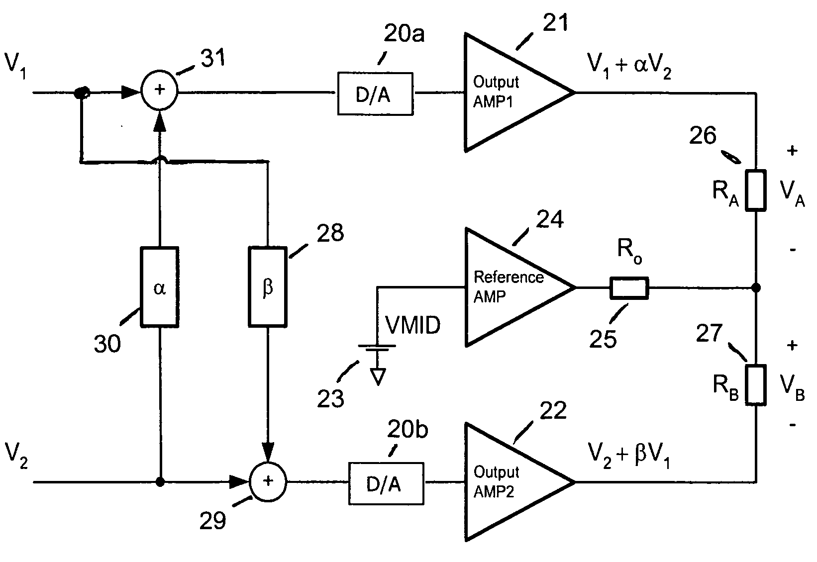
[0026]FIG. 3 is a simplified schematic drawing of an amplifier configuration in accordance with the present invention. In this embodiment, the signal from each channel is added to the other channel on the input of the output amplifiers. The signal VI is converted by a digital-to-analog (D / A) converter 20a and fed into a first single-ended output amplifier (Output AMPL1) 21, and the signal V2 is converted by a D / A converter 20b and fed into a second single-ended output amplifier (Output AMP2) 22. A reference voltage supply (VMID) 23 is implemented as an input to a reference amplifier (Reference AMP) 24. The Reference AMP has an internal output impedance R0 25, and generates a reference signal, which may be a reference DC voltage level. A first output load (RA) 26 is connected between Output AMP121 and the Reference AMP. A voltage drop VA is associated with the first output load RA. A second output load (RB) 27 is connected between Output AMP222 and the Reference AMP. A voltage drop V...

second embodiment

[0036]FIG. 4 is a simplified schematic drawing of an amplifier configuration in accordance with the present invention. In this embodiment, the signals from both channels are added on the input of the reference amplifier. The signals V1 and V2 are split prior to their respective Output AMPs, and are routed through an adder 33 and a gain function a 34. A suitable DC bias, VMID 23, is added to the adjusted sum before voltage V0 is applied to the Reference AMP 24. The Reference AMP generates a reference signal, which may be a reference DC voltage level. Note that the added DC bias may be zero, depending on the values of V1 and V2, respectively.

[0037]Like in the first embodiment, it can be shown that this embodiment also results in crosstalk equal to to −R0 / R=−Rint / RL. The calculations below begin by showing that VA and VB are the signals that will appear over the resistive loads RA and RB, respectively. Without loss of generality, all amplifiers are assumed to have 0 dB gain.

{VA=V1RARA+...


PUM


Abstract

A method and ASIC for canceling crosstalk between a first stereo channel and a second stereo channel, wherein a first signal is input to a first output amplifier for the first channel, and a second signal is input to a second output amplifier for the second channel, and an output load for each output amplifier is connected between each output amplifier and a reference amplifier. In one embodiment, the first and second signals are split prior to inputting the signals to the first and second output amplifiers, and a gain-adjusted portion of each signal is added to the other signal on the inputs of the output amplifiers. In another embodiment, the first and second input signals are again split into two paths each. While a first path of each signal is inputted to each signal's respective output amplifier, the second paths of the first and second signals are adding together. The resulting sum is adjusted by a gain function, biased by a suitable DC voltage, and input to the reference amplifier.

Description

BACKGROUND OF THE INVENTION[0001]The present invention relates to systems for amplifying electronic signals. More particularly, and not by way of limitation, the present invention is directed to a system and method for canceling crosstalk between multiple channels using load impedance measurements.[0002]Driving a stereo headset is a common requirement in today's mobile phones. There is a requirement to minimize the number of pins in the headset connector, and also to adhere to the standard headset connector found on most home music equipments. Typically, the standard headset has a three-terminal connector with left, right, and ground terminals. No DC current is allowed to flow through the headset. This requires the left and right signals to be an AC signal with a zero-volt DC offset. Such a signal may be generated using an amplifier with a positive and negative voltage supply. However, a negative supply is not readily available in a device operated by a single battery.[0003]FIG. 1A ...

Claims


Application Information

Patent Timeline
Patent Type & Authority Applications(United States)
IPC IPC(8): H04H5/00
CPCH04S1/00H04S7/30H04S7/00H04S1/005H04R5/033
Inventor HOLMSTROM, MICHAELEDHOLM, BENGTMATTISSON, SVEN
Owner TELEFON AB LM ERICSSON (PUBL)
Why Eureka
Try Eureka