Wiring board with lead pins, and lead pin

Active Publication Date: 2008-01-10
SHINKO ELECTRIC IND CO LTD
View PDF3 Cites 24 Cited by
  • Summary
  • Abstract
  • Description
  • Claims
  • Application Information

AI Technical Summary

Benefits of technology

[0023] In the wiring board with lead pins according to the present invention, the lead pins are assuredly attached to the electrode pads formed on the wiring board. When the lead pins are attached to the electrode pads by using the conductive agent, voids can be prevented from remaining in attached portions of the lead pi

Problems solved by technology

However, when the application amount of the solder paste is reduced, a problem arises that a bonding strength of the lead pins 5 and the electrode pads 12 is deteriorated.
However, in the case where the head portions of the lead pins are formed in flat planes, although the grooves are provided in the head portions, an operation for releasing the volatiliz

Method used


Image

  • Wiring board with lead pins, and lead pin
  • Wiring board with lead pins, and lead pin
  • Wiring board with lead pins, and lead pin

Examples


Embodiment Construction

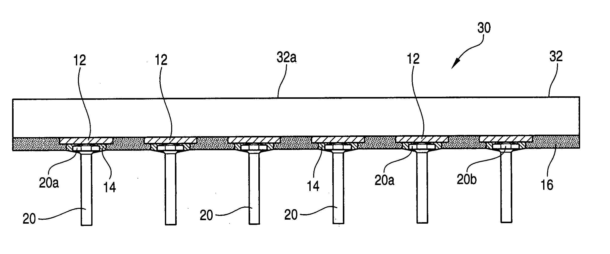
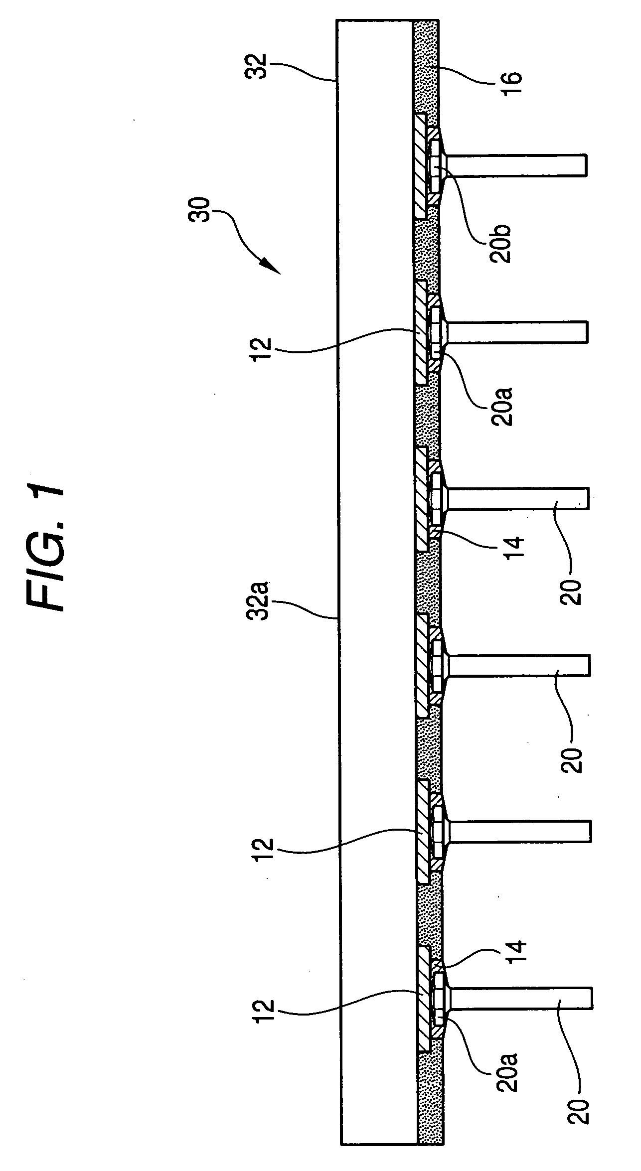
[0031]FIG. 1 is a partial sectional view showing a structure of a wiring board with lead pins according to an embodiment of the present invention. In a wiring board 30 with lead pins according to this embodiment, one surface of a wiring board 32 is formed as a mounting portion 32a for mounting a semiconductor element or the like. On the other surface of the wiring board 32, electrode pads 12 are provided and lead pins 20 are attached to the electrode pads 12. On the mounting portion 32a, a wiring pattern for mounting the semiconductor element or circuit components such as resistance is formed. A structure of the wiring pattern formed on the mounting portion 32a is the same as that of an ordinary wiring board. In FIG. 1, the structure of the mounting portion 32a is omitted.

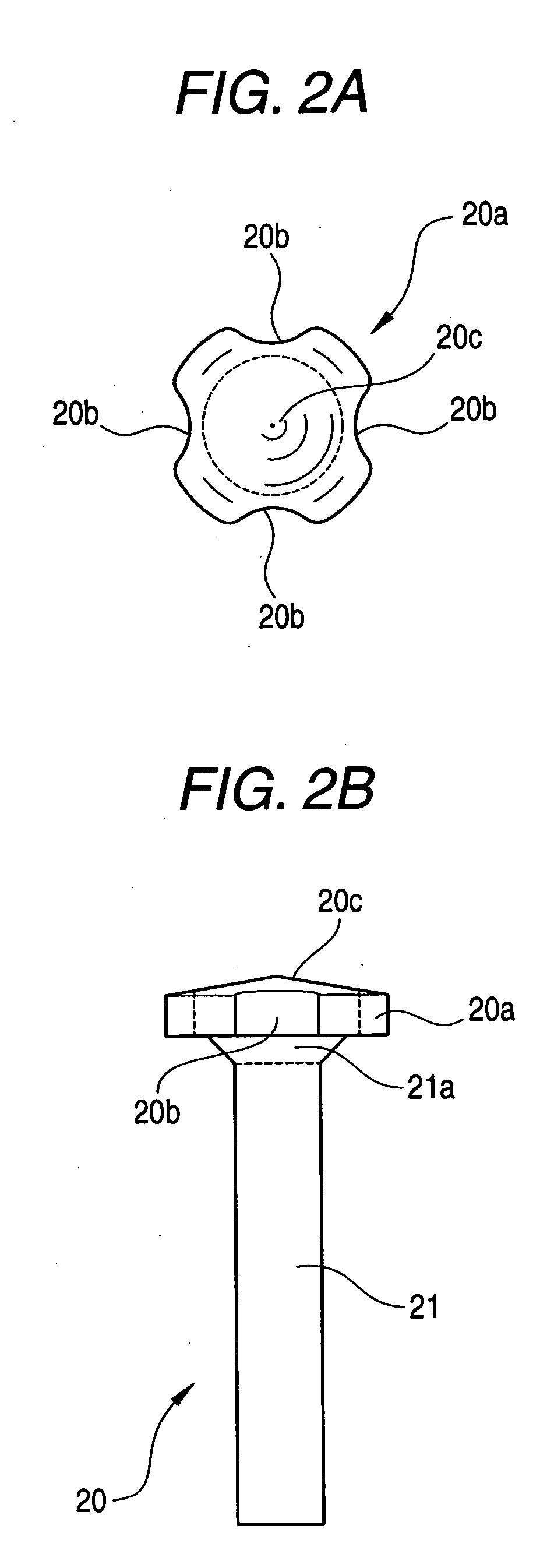
[0032] The other surface of the wiring board 32 is coated with a solder resist 16 as a protective coating except surfaces of the electrode pads 12 to which the lead pins 20 are attached. The electrode pads 12 are ...


PUM


Abstract

A wiring board with lead pins having high reliability is provided. When the lead pins are attached to electrode pads, the lead pins are attached to the electrode pads without leaving voids in a conductive agent, and bonding strength of the lead pins are improved. When the wiring board to which the lead pins are attached is reheated, the lead pins are prevented from being inclined or shifted from their normal positions. In the wiring board with lead pins formed by attaching head portions of the lead pins to the electrode pads formed on the wiring board through the conductive agent, the lead pin has notch portions are formed in cut-out shapes in peripheral edge portion of the disk shaped head portion.

Description

[0001] This application claims foreign priority based on Japanese Patent application No. 2005-166455, filed Jun. 7, 2005, the contents of which is incorporated herein by reference in its entirety. BACKGROUND OF THE INVENTION [0002] 1. Field of the Invention [0003] The present invention relates to a wiring board with lead pins and a lead pin, and more particularly to a wiring board with lead pins and a lead pin used for the wiring board, the wiring board being formed by attaching the lead pins to electrode pads formed on a surface of the board such as a pin grid array (PGA) type wiring board. [0004] 2. Description of the Related Art [0005]FIGS. 6A to 6C show a related manufacturing process for manufacturing a wiring board with lead pins by attaching lead pins 5 to electrode pads 12 formed on a surface of a wiring board 10. FIG. 6A shows a state in which solder paste 14a is applied to surfaces of the electrode pads 12 formed on the wiring board 10, and the lead pins 5 are arranged so ...

Claims


Application Information

Patent Timeline
IPC IPC(8): H01R12/00
CPCH01L2924/15312H01R43/0256H05K3/3426H05K2201/10318H01L2924/0002H01L2924/00Y02P70/50
Inventor IDE, KAZUHIKOMOTODA, HIROYUKIFURIHATA, YOSHINORI
Owner SHINKO ELECTRIC IND CO LTD
Why Eureka
Try Eureka