Wiring substrate, semiconductor device, and method of manufacturing the same

a technology of wiring substrate and semiconductor device, which is applied in the direction of printed circuit manufacturing, printed circuit stress/warp reduction, printed circuit aspects, etc., can solve the problems of difficult to reduce the pitch between the external electrode terminals, difficult to reduce the pitch of the external electrode terminal, and difficult to control the amount of side etching. , to achieve the effect of stable mounting, improved productivity and appropriate transfer

Inactive Publication Date: 2008-01-17
RENESAS ELECTRONICS CORP +1
View PDF2 Cites 94 Cited by
  • Summary
  • Abstract
  • Description
  • Claims
  • Application Information

AI Technical Summary

Benefits of technology

[0059]The present invention can provide a wiring substrate on which a semiconductor chip can be appropriately mounted. The present invention can also provide a method of manufacturing a semiconductor device which enables a semiconductor chip to be stably mounted and allows a substrate with the semiconductor chip mounted thereon to be more appropriately transferred, improving productivity.

Problems solved by technology

However, a problem with the built-up printed substrate is that because of the use of a glass epoxy printed substrate of low heat resistance as the base core substrate, deformation such as warpage or waviness is apt to occur in the substrate by heating during the formation of a multilayer structure or the mounting of a semiconductor chip.
However, since in this wiring substrate for packaging, the external electrode terminals 508 are formed by etching the metal sheet 501, it is difficult to reduce the pitch between the external electrode terminals 508 owing to limits to the control of the amount of side etching.
This disadvantageously increases the likelihood of open faults and prevents the substrate from being sufficiently reliable.
If a wiring substrate with no semiconductor chip mounted yet is warped on a stage, the wiring substrate may be misaligned with respect to the stage when placed on and fixed to the stage, or transferring the wiring substrate may become difficult.
This unfortunately degrades the reliability and productivity of products.
Even if a wiring substrate is placed on a stage using a method such as the one described in Patent Document 6, the substrate with a semiconductor chip mounted thereon may disadvantageously be warped with its central part raised along the transfer direction.
When the substrate is warped with its central part raised, during transfer thereof, the substrate with the chip mounted thereon may disadvantageously comes into contact with a member that is located over a transfer route such as a substrate holding guide or a heating cover.

Method used


Image

  • Wiring substrate, semiconductor device, and method of manufacturing the same
  • Wiring substrate, semiconductor device, and method of manufacturing the same
  • Wiring substrate, semiconductor device, and method of manufacturing the same

Examples


Embodiment Construction

[0074]Examples in accordance with preferred embodiments of the present invention will be described below.

Interconnection Structure

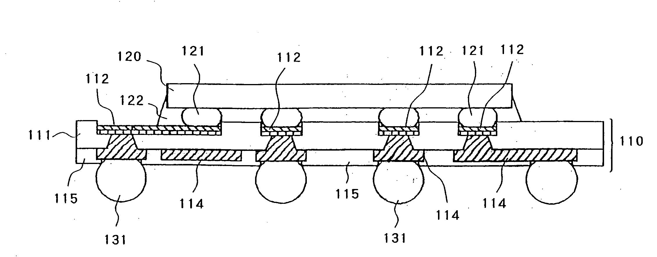
[0075]First, with reference to FIG. 1, description will be given of the basic interconnection structure of a wiring substrate in accordance with an embodiment of the present invention.

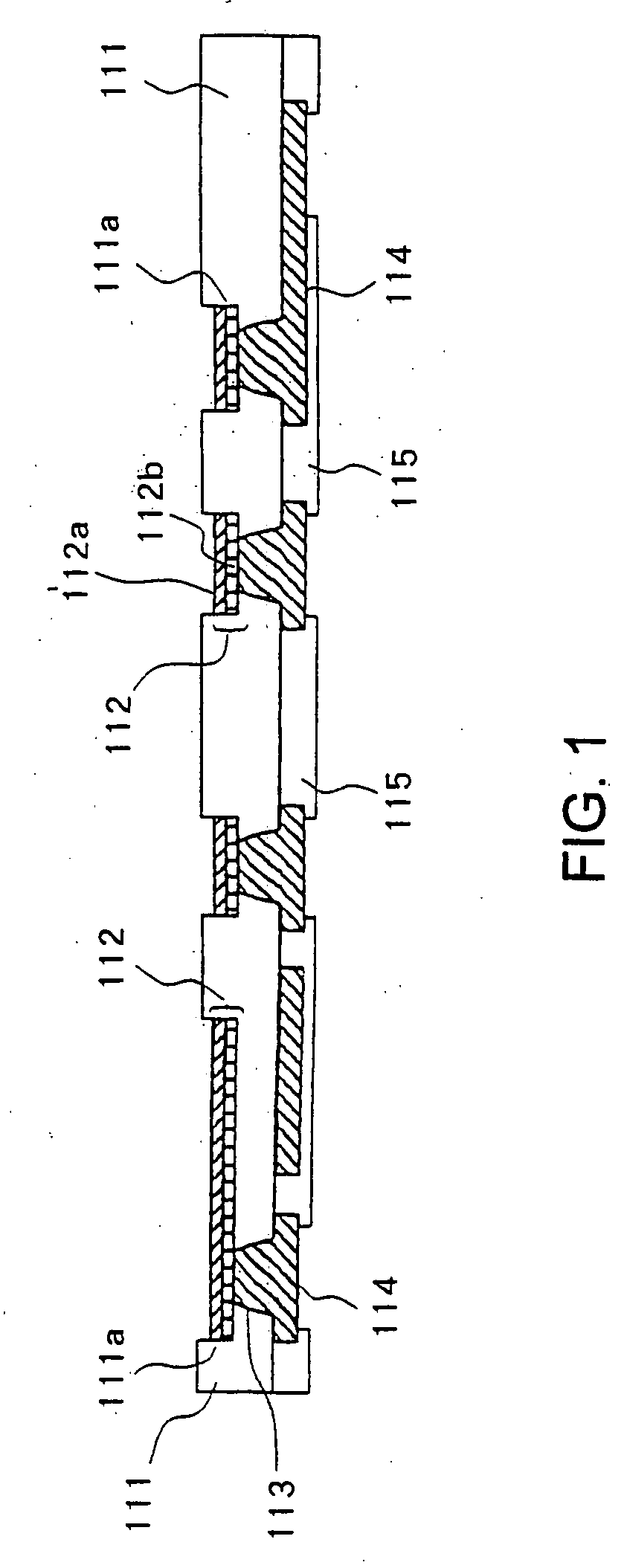
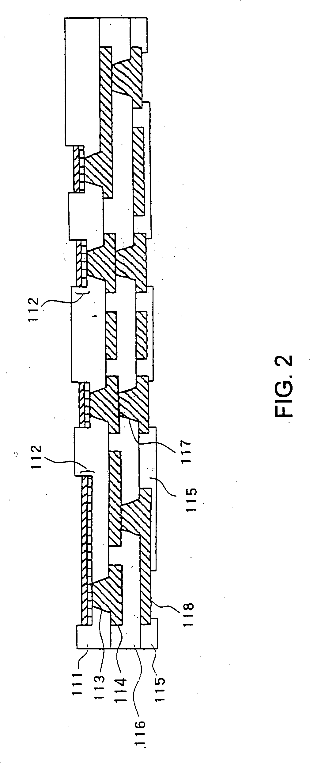
[0076]A wiring substrate in accordance with the embodiment has a base insulating film 111, an upper layer interconnection 112 (112a, 112b) provided on a top surface side of the base insulating film, a conductor provided in a via hole 113 formed in the base insulating film, and a lower layer interconnection 114 connected to the upper layer interconnection via the via conductor and formed on a bottom surface of the base insulating film. The upper layer interconnection 112 is provided in a sunken section 111a formed in a top surface of the base insulating film 111. A solder resist layer 115 is formed on a bottom surface side of the base insulating film 111 so as to expose a par...


PUM


Abstract

A wiring substrate includes a base insulating film, a first interconnection formed on a top surface side of the base insulating film, a via conductor provided in a via hole formed in the base insulating film, and a second interconnection provided on a bottom surface side of the base insulating film, the second interconnection being connected to the first interconnection via the via conductor. The wiring substrate includes divided-substrate-unit regions, in each of which the first interconnection, the via conductor, and the second interconnection are formed. The wiring substrate includes a warpage-controlling pattern on the base insulating film, and has a warped shape such that when the wiring substrate is left at rest on a horizontal plate, at least a central part of each side of a plane surface of the substrate contacts the horizontal plate, with both ends of the side raised, where each of the sides extends along a second direction perpendicular to a first direction in the plane surface of the substrate.

Description

BACKGROUND OF THE INVENTION[0001]1. Field of the Invention[0002]The present invention relates to a wiring substrate on which a semiconductor chip is mounted, a semiconductor device using the wiring substrate, and a method of manufacturing the semiconductor device.[0003]2. Description of the Related Art[0004]Recent semiconductor devices with improved performance, increased number of functions, and increased density have an accordingly increased number of terminals arranged at a reduced pitch. Thus, wiring substrates for packaging on which semiconductor devices are mounted have been desired to have more densely arranged interconnections of further reduced sizes.[0005]Built-up printed substrates, a kind of multilayer wiring substrate, have been commonly used as wiring substrates for packaging. In the built-up printed substrate, resin layers are formed on a top surface and a bottom surface of a glass epoxy printed substrate which serves as a base core substrate and on which interconnect...

Claims


Application Information

Patent Timeline
Patent Type & Authority Applications(United States)
IPC IPC(8): H01L23/52H01L21/4763
CPCH01L21/4846H01L21/563H01L2924/10253H01L21/6835H01L23/13H01L23/49816H01L23/49827H01L2224/16H01L2924/01046H01L2924/01078H01L2924/01079H01L2924/09701H01L2924/15311H05K1/0271H05K3/205H05K3/4644H05K2201/09018H05K2201/09481H05K2201/09781H01L2924/01019H01L2924/00H01L2224/16235H01L2224/16237H01L2924/00014H01L2224/16225H01L2224/32225H01L2224/73204H01L2924/00011H01L2224/0401H01L23/12H05K3/46
Inventor TSUKANO, JUNOGAWA, KENTAMAEDA, TAKEHIKOYAMAMICHI, SHINTAROKIKUCHI, KATSUMI
Owner RENESAS ELECTRONICS CORP
Why Eureka
Try Eureka