Method for the manufacture of solar panels and special transport carrier

a technology of solar panels and transport carriers, applied in the field of solar panel manufacturing and special transport carriers, can solve the problems of inability to meet the requirements of yield criteria, no functionality, contamination of parts, etc., and achieve the effect of reducing production costs, reducing production costs, and reducing production costs

Inactive Publication Date: 2008-01-17
IBM CORP
View PDF11 Cites 15 Cited by
  • Summary
  • Abstract
  • Description
  • Claims
  • Application Information

AI Technical Summary

Benefits of technology

[0014]It is therefore an object of the present invention to provide a method for the manu

Problems solved by technology

However, when manufacturing wafers and/or dies, scrap parts will occur due to contamination, physica

Method used


Image

  • Method for the manufacture of solar panels and special transport carrier
  • Method for the manufacture of solar panels and special transport carrier
  • Method for the manufacture of solar panels and special transport carrier

Examples


Embodiment Construction

[0025]As has already been mentioned above, shortage of raw material for solar cell manufacturers requires new solutions to increase the supply. In addition, a process has to be enabled which allows obtaining raw panels for solar cells on a cost competitive level. Furthermore, the new process, using semiconductor scrap wafers and dies, must assure that the required specification limits for solar panels are achieved.

[0026]The present invention provides a recycling process that is able to prevent disposal of scrap parts and related costs. The process can be used with 300 mm wafers as well as 200 mm wafers and, in addition, with all types of wafer dies. Thus, the inventive process is able to use scrapped wafers as well as sufficient large scrapped dies for photovoltaic solar element production.

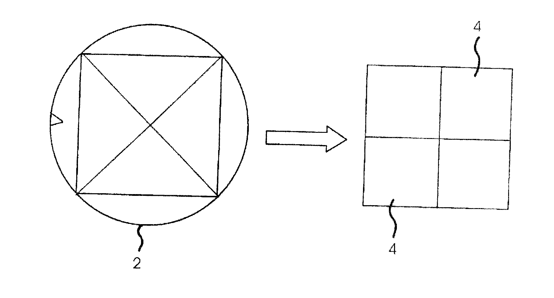
[0027]According to the invention, wafer scrap from 200 mm as well as 300 mm semiconductor manufacturing can be used to make square panels for solar cell production. As is shown in FIG. 1, in the c...


PUM


Abstract

A method for the manufacture of solar panels from scrapped wafers and/or scrapped dies is provided, including the following steps: identifying scrap wafers and/or scrap dies; cleaning and removing remaining structures from the surface of the wafers/dies; grinding both surfaces of the wafers/dies down to a required thickness; doping the wafers/dies; and further processing the wafers/dies using a solar panel manufacturing method.

Description

CROSS REFERENCE TO RELATED APPLICATIONS[0001]This application is related to German Patent Application No. 06116972.8, filed Jul. 11, 2006.FIELD OF THE INVENTION[0002]The present invention relates in general to a method for the manufacture of solar panels. More specifically, the invention relates to a recycle process of semiconductor wafers and dies. In addition, the present invention is concerned with a special transport carrier used during the recycle process.BACKGROUND OF THE INVENTION[0003]A solar panel is a flat collection of solar cells or solar thermal collectors used for converting solar energy into electricity or heat. The term “solar panel” can be applied to either solar hot water panels (usually used for providing domestic hot water) or solar photovoltaic panels (providing electricity). In the following, the main focus will be on solar photovoltaic panels.[0004]A solar cell or photovoltaic cell is a semiconductor device consisting of a large-area p-n junction diode, which ...

Claims


Application Information

Patent Timeline
IPC IPC(8): H01L21/00
CPCC01B33/037C01B33/02
Inventor HAAG, MICHAELKALTENBACH, MICHAELKLEEMANN, UDOKRAUSE, RAINERMURRAY, DOUGLAS J.PFEIFFER, GERDSCHMIDT, MARKUS
Owner IBM CORP
Why Eureka
Try Eureka