Defect Inspection Method and Apparatus

a technology of defect inspection and inspection method, applied in the direction of mechanical roughness/irregularity measurement, optical radiation measurement, instruments, etc., can solve the problems of low sensitivity, false judgment, inability to detect defects, etc., to reduce brightness unevenness, high processing speed, and high sensitivity

Active Publication Date: 2008-01-17
HITACHI HIGH-TECH CORP
View PDF3 Cites 79 Cited by
  • Summary
  • Abstract
  • Description
  • Claims
  • Application Information

AI Technical Summary

Benefits of technology

[0022] The aspect of the invention for solving the above-described first problems of the conventional inspection techniques relates to a pattern inspection apparatus which compares images of regions, corresponding to each other, of patterns that are formed so as to be identical and judges that non-coincident portions of the image are defects. This aspect of the invention is intended to realize a defect inspection which can reduce brightness unevenness between comparison images due to differences in film thickness, differences in pattern thickness, or the like and can detect, keeping high processing speed and high sensitivity, defects desired by a user that are buried in noise or defects that need not be detected in such a manner as to flexibly accommodate even a case that the appearance varies depending on the defect type.
[0023] In a pattern inspection apparatus which compares images of regions, corresponding to each other, of patterns that are formed so as to be identical and judges that non-coincident portions of the image are defects, this aspect of the invention makes it possible to lower the influence of brightness unevenness between comparison images due to differences in film thickness, differences in pattern thickness, or the like and to enable a high-sensitivity defect inspection merely by simple parameter setting.
[0024] This aspect of the invention allows a defect inspection apparatus to perform a high-sensitivity defect inspection capable of accommodating a variety of defects by calculating feature quantities of pixels of comparison images and employing, as defect candidates, pixels having excessively deviated values in a feature space.
[0025] This aspect of the invention also makes it possible to increase the number of detectable defect types and detect various defects with high sensitivity by unifying, at each stage, pieces of information that are output from plural detection systems. With the above-described features, this aspect of the invention makes it possible to detect fatal defects with high sensitivity even in the case where the inspection subject is a semiconductor wafer and brightness differences occur between the same patterns of images due to differences in film thickness in a wafer.
[0026] Furthermore, this aspect of the invention enables high-speed, high-sensitivity defect inspection in which pieces of processing can be assigned to CPUs freely by employing, for a defect detection processing section, a system configuration comprising a parent CPU, plural child CPUs, and oppositely-directed data transfer buses.
[0027] On the other hand, Conventional techniques 1-8 have a problem that in an irregular circuit pattern portion a signal representing a defect is overlooked because of scattered light from the pattern and the sensitivity is thereby lowered.

Problems solved by technology

However, these portions should not be detected as defects; that is, this is a false judgment.
However, this lowers the sensitivity and makes it unable to detect defects whose difference values are approximately equal to the threshold value.
In conventional brightness-based comparative inspections, such brightness variation causes noise during an inspection.
Although appearance inspections are required to extract defects desired by a user from an enormous number of defects, it is difficult to satisfy this requirement by the above-mentioned comparison between luminance differences and a threshold value.

Method used


Image

  • Defect Inspection Method and Apparatus
  • Defect Inspection Method and Apparatus
  • Defect Inspection Method and Apparatus

Examples


embodiment 1

of the Invention for Solving the First Problems

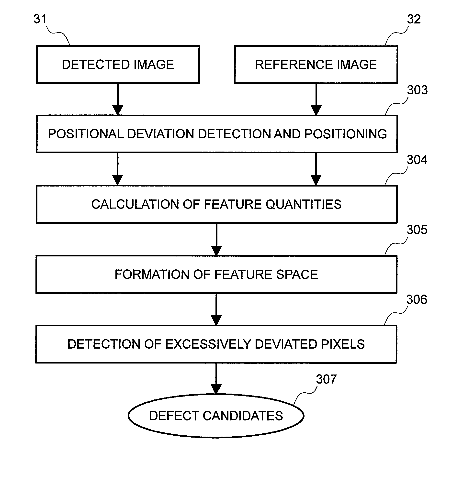
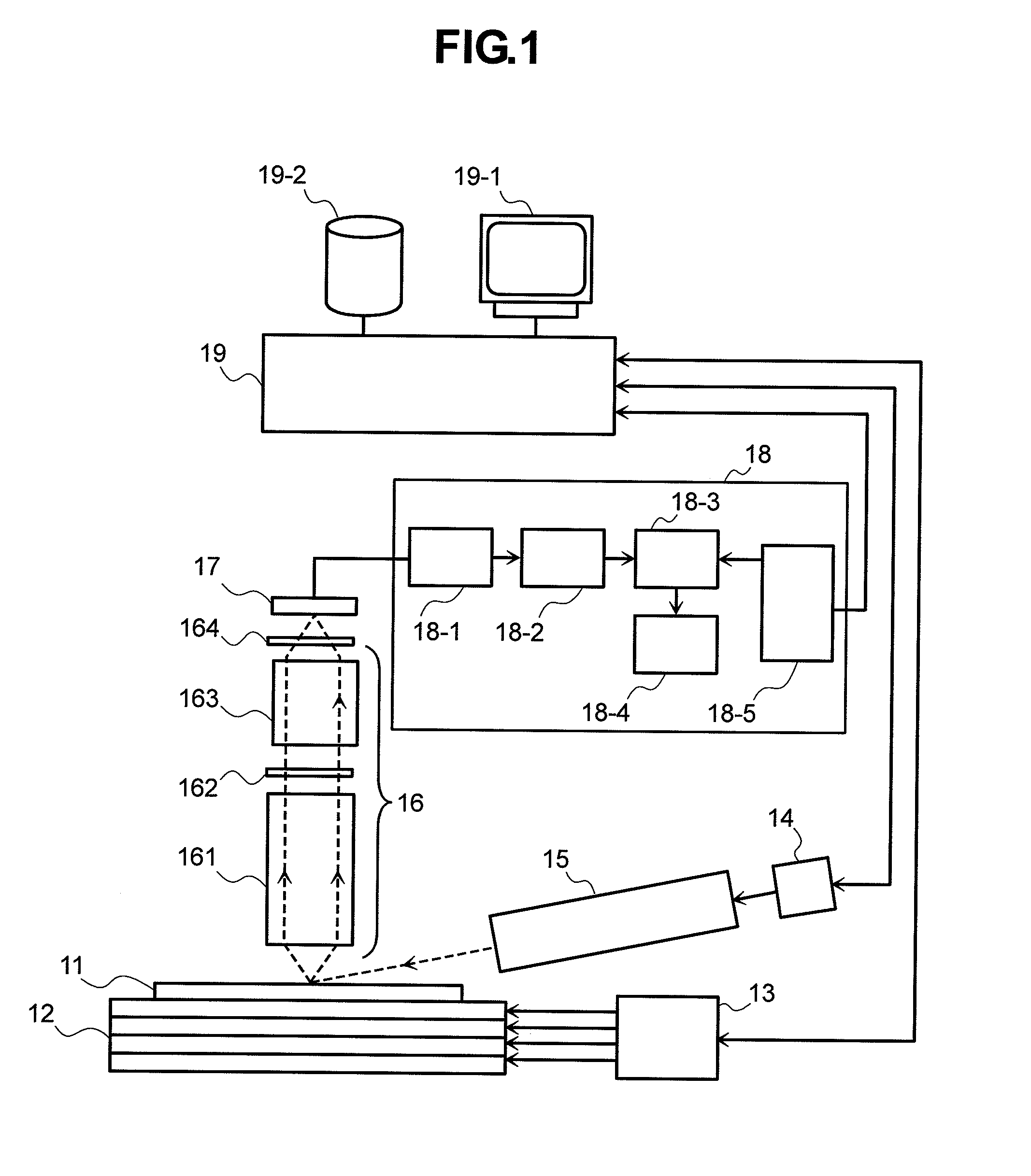
[0075] A first embodiment will be described below which is a defect inspection method employed by a defect inspection apparatus for semiconductor wafers which uses dark-field illumination. FIG. 1 shows the configuration of an exemplary defect inspection apparatus using dark-field illumination. Symbol 11 denotes a sample (an inspection subject such as a semiconductor wafer), symbol 12 denotes a stage capable of being moved and rotated in the XY-plane and being moved in the Z-direction (height direction) while being mounted with the sample 11, and symbol 13 denotes a mechanical controller for driving the stage 12. Symbol 14 denotes a light source for emitting laser light and symbol 15 denotes an illumination optical system. Laser light emitted from the light source 14 is applied to the sample 11 via the illumination optical system 15. Scattered light coming from the sample is 11 image-formed by an upper detection system 16, and a resultin...

embodiment 2

of the Invention for Solving the First Problems

[0101] A second embodiment is directed to another defect inspection method in which the image processing system having the system configuration described in the first embodiment is employed and plural detection optical systems for detecting images are provided. The inspection apparatus of FIG. 9 is configured in such a manner that an oblique detection optical system 90 is added to the defect inspection apparatus of FIG. 1 which uses dark-field illumination (i.e., two detection optical systems are provided). Like the upper detection system 16, the oblique detection optical system 90 is composed of an objective lens 901, a spatial filter 902, an image-forming lens 903, and an optical filter 904. Scattered light coming from a sample 11 is image-formed via the objective lens 901, the spatial filter 902, the image-forming lens 903, and the optical filter 904, and a resulting optical image is detected by an image sensor 91 and thereby convert...

embodiment 3

of the Invention for Solving the Second Problems

[0136]FIG. 20 shows the configuration of a defect inspection apparatus according to the third embodiment. This defect inspection apparatus is composed of a light source 0-1, an illumination optical system 0-100, an inspection subject substrate W, an objective lens 0-3a, a spatial filter 0-4a, an image-forming lens 0-5a, a polarization detecting section 0-200a, a signal processing section 0-300, a total control section 0-6, a display section 0-7, a computing section 0-8, a storage section 0-9, an X-Y-Z-θ stage driver 0-10, an X-Y-Z-θ stage 0-11, and a light source driver 0-12. The light source 0-1, the illumination optical system 0-100, the objective lens 0-3a, the spatial filter 0-4a, the image-forming lens 0-5a, and the polarization detecting section 0-200a constitute an optical system 0-1000.

[0137] The operation will be outlined below. Light emitted from the light source 0-1 is applied to the inspection subject substrate W via the i...


PUM

PropertyMeasurementUnit
thicknessaaaaaaaaaa
azimuth angleaaaaaaaaaa

Abstract

A pattern inspection apparatus which compares images of regions, corresponding to each other, of patterns that are formed so as to be identical and judges that non-coincident portions in the images are defects. The pattern inspection apparatus is equipped with an image comparing section which plots individual pixels of an inspection subject image in a feature space and detects excessively deviated points in the feature space as defects. Defects can be detected correctly even when the same patterns in images have a brightness difference due to a difference in the thickness of a film formed on a wafer.

Description

BACKGROUND OF THE INVENTION [0001] The invention disclosed in this specification relates to an inspection of comparing an image of a subject obtained by using light, laser light, or an electron beam with a reference image and detecting fine-pattern defects, foreign particles, etc. on the basis of a result of the comparison. In particular, the invention relates to a defect inspection method and apparatus which are suitable for an appearance inspection of semiconductor wafers, TFTs, photomasks, etc. [0002] Among conventional techniques for detecting defects by comparing an inspection subject image with a reference image is a method disclosed in JP-A-5-264467 (Patent document 1). [0003] In this technique, repetitive patterns that are arranged regularly on an inspection subject sample are shot sequentially and each resulting image is compared with an image that has been delayed by a time corresponding to a pattern repetition pitch. Non-coincident portions are detected as defects. This k...

Claims


Application Information

Patent Timeline
Patent Type & Authority Applications(United States)
IPC IPC(8): G06F19/00G01J4/00G01N21/00
CPCG01N21/4738G01N21/956G01N21/9501
Inventor URANO, YUTAHAMAMATSU, AKIRAMAEDA, SHUNJISAKAI, KAORU
Owner HITACHI HIGH-TECH CORP
Why Eureka
Try Eureka