Method for measuring thin layers in solid state devices

a solid-state device and thin-layer technology, applied in the direction of mechanical measuring arrangements, instruments, using mechanical means, etc., can solve the problems of destroying, time-consuming methods, and inability to optically measure the thickness of the bonding layer,

Inactive Publication Date: 2008-01-24
IBM CORP
View PDF9 Cites 18 Cited by
  • Summary
  • Abstract
  • Description
  • Claims
  • Application Information

AI Technical Summary

Benefits of technology

[0009]The method of the present invention thus will enable one to determine the precise thickness measurement of such an intermediate bonding layer regardless of a thickness of the bonding layer.

Problems solved by technology

The complexity and compactness of present day electronic devices requires the inclusion of thin bonding layers in various circuit configurations such as may be used to secure a semiconductor device to a heat sink or cap.
An early but destructive, time-consuming method requires the cutting of the device transverse to the thickness of the buried layer and then optically measuring the thickness of the exposed buried layer.
However, certain assemblies make optical measurements of the bonding layer thickness impossible.
Recently, Fast Fourier Transform (FFT) methods have also been employed to measure thin layer thicknesses, however these methods have yet to be successfully and robustly applied to thin bonding layers.
By thin layers it is meant that the reflected acoustic signals returning from the layer are usually merged into one single echo making thickness measurements by conventional techniques very imprecise or impossible, for the reflections from both the top and the bottom of such thin bonding layers overlap another, such that the signal reflected from the top of the bonding layer cannot be differentiated from the signal reflected from the bottom of the bonding layer.
As newer, smaller semiconductor devices require bonding layers that are thinner than the threshold thickness where top and bottom echoes begin to separate, the prior art techniques are unsatisfactory and the art has been seeking a measurement technique that would provide for accurate non-destructive measuring of such thin bonding layers.

Method used


Image

  • Method for measuring thin layers in solid state devices
  • Method for measuring thin layers in solid state devices
  • Method for measuring thin layers in solid state devices

Examples


Embodiment Construction

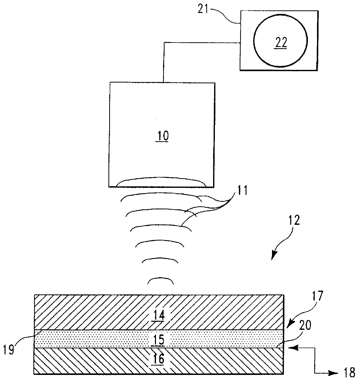
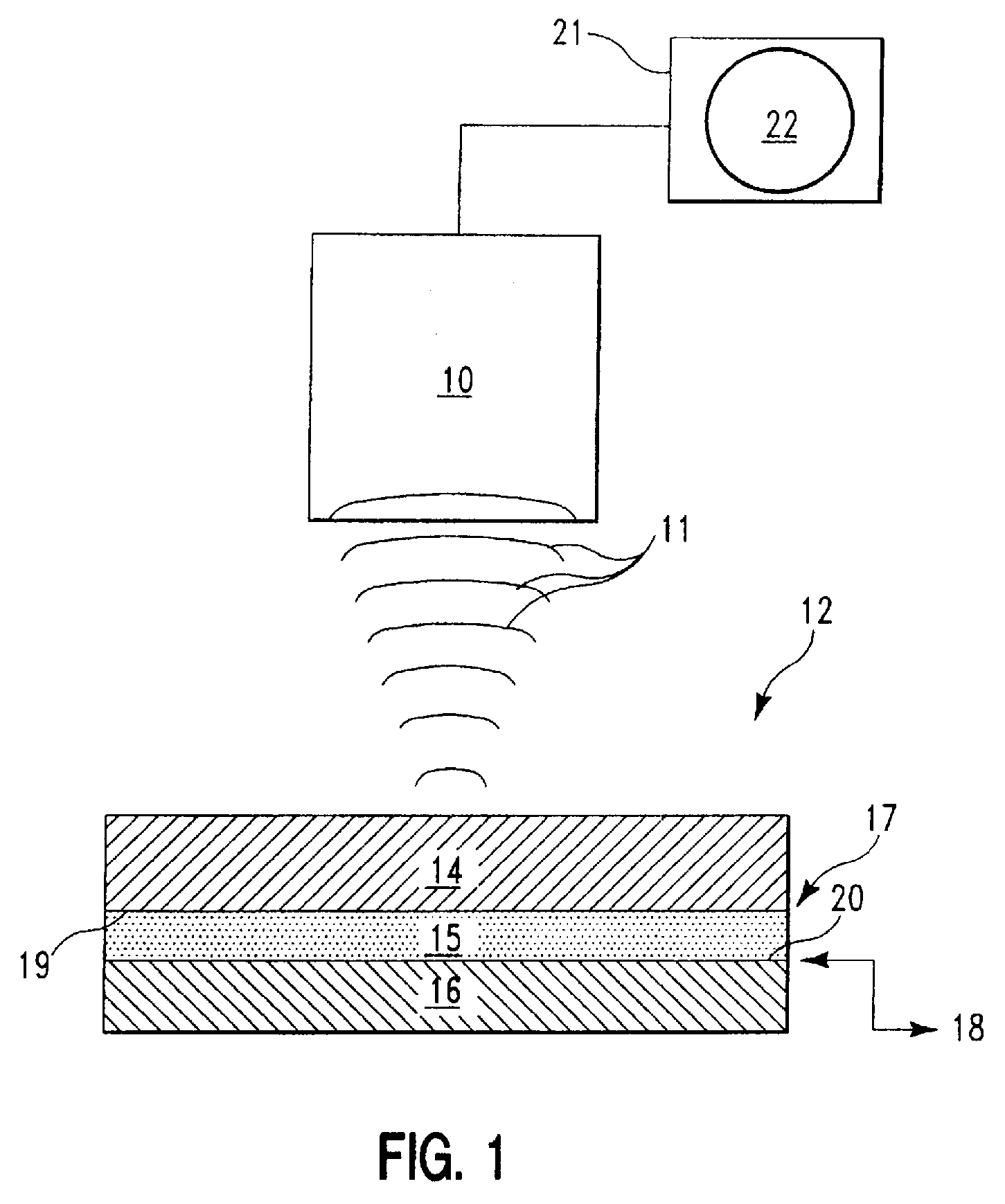
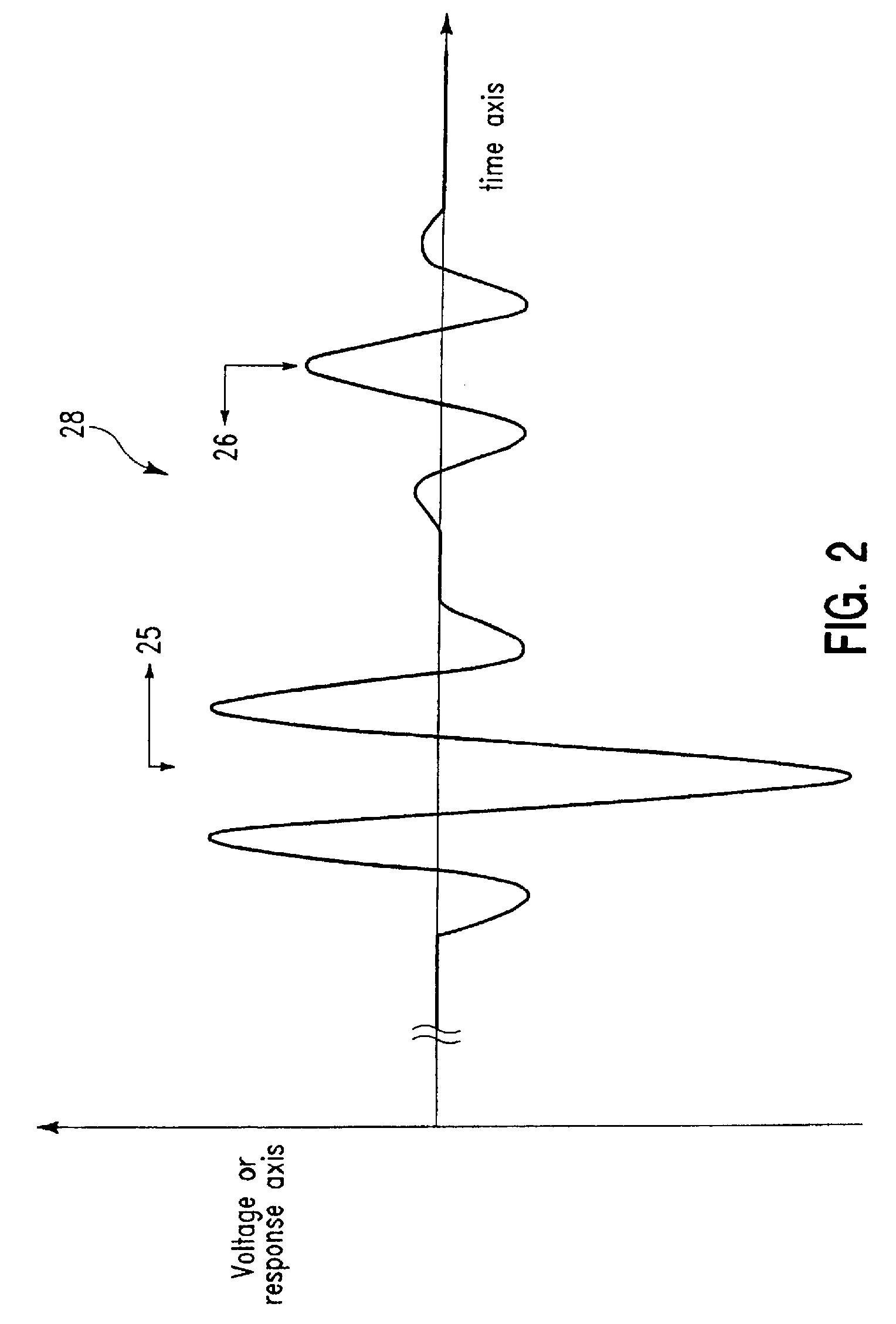
[0023]FIG. 1 schematically illustrates a commercially available acoustic microscope 10 coupled to a computer 21 provided with an oscilloscope display 22. The microscope 10 is designed to transmit an acoustic wave 11 to a layered body 12 and to receive and process the echoes reflected there from. The layered body 12 is, for example, comprised of an upper layer 14 formed of a first material such as SiSiC, that is secured to a lower layer 16, formed, for example, of silicon, by an intermediate bonding layer 15, formed, for example, of a bonding material such as a thermal paste. More particularly, the bonding layer 15 forms a reflective or echoing interface 17 with the bottom surface 19 of the upper layer 14 and a subsequent reflective or echoing interface 18 with the top surface 20 of the lower layer 16. When an acoustic wave is applied to the body 12 the wave is reflected from each of the two interfaces 17 and 18 as shown in FIG. 2. Such reflected waves will hereinafter be referred to...


PUM


Abstract

A method of using acoustic signals in the form of waves or pulses to non-destructively measure the thickness of a bonding layer sandwiched between and bonding together overlying and underlying materials different from the bonding layer especially when the thickness of the bonding layer is so small that the features (maxima, minima, time position) of the echo from the interface of the bonding layer and the overlying material is indistinguishable, i.e., not independently observable from the features (maxima, minima, time position) of the echo from the interface of the bonding layer and the underlying material.

Description

FIELD OF THE INVENTION[0001]This invention generally relates to a reflective acoustic microscopy method for measuring the thickness of bonding layers in a body, used to bond together elements especially in solid-state or microelectronic devices.BACKGROUND OF THE INVENTION[0002]The complexity and compactness of present day electronic devices requires the inclusion of thin bonding layers in various circuit configurations such as may be used to secure a semiconductor device to a heat sink or cap. Measurement of the thickness of such bonding layers is essential to assure that the devices will not only function properly but also will operate within their design parameters especially as regards the device heat transfer requirements,[0003]Several methods presently exist for measuring the thickness of such bonding layers. An early but destructive, time-consuming method requires the cutting of the device transverse to the thickness of the buried layer and then optically measuring the thickne...

Claims


Application Information

Patent Timeline
Patent Type & Authority Applications(United States)
IPC IPC(8): G01B17/02
CPCG01B17/02
Inventor BLANDER, ALEXANDREBRASSARD, RICHARDSAVARD, CARLSYLVESTRE, JULIEN
Owner IBM CORP
Why Eureka
Try Eureka