
Semiconductor device and manufacturing method of the same

a semiconductor and manufacturing method technology, applied in semiconductor devices, semiconductor/solid-state device details, electrical devices, etc., can solve problems such as mechanical defects in semiconductor substrates and reduce production efficiency

Active Publication Date: 2008-01-31
SEMICON COMPONENTS IND LLC
View PDF21 Cites 27 Cited by
  • Summary
  • Abstract
  • Description
  • Claims
  • Application Information

AI Technical Summary

Benefits of technology

[0019] This invention is directed to solve the problems addressed above and has following features. The invention provides a method of manufacturing a semiconductor device, including: forming a mask layer selectively on a front surface of a semiconductor substrate; forming an opening in the semiconductor substrate by dry-etching the semiconductor substrate using the mask layer as a mask with an etcher; and removing the mask layer with the etcher with the semiconductor substrate still placed in the etcher.

Problems solved by technology

Therefore, when the ashing process is to be performed after the etching process or the etching process is to be performed after the ashing process, it is necessary to transfer the semiconductor substrate 100 each time, thereby largely reducing production efficiency.
Furthermore, a mechanical defect may occur in the semiconductor substrate 100 during the transfer.

Method used


Image

  • Semiconductor device and manufacturing method of the same
  • Semiconductor device and manufacturing method of the same
  • Semiconductor device and manufacturing method of the same

Examples


Embodiment Construction

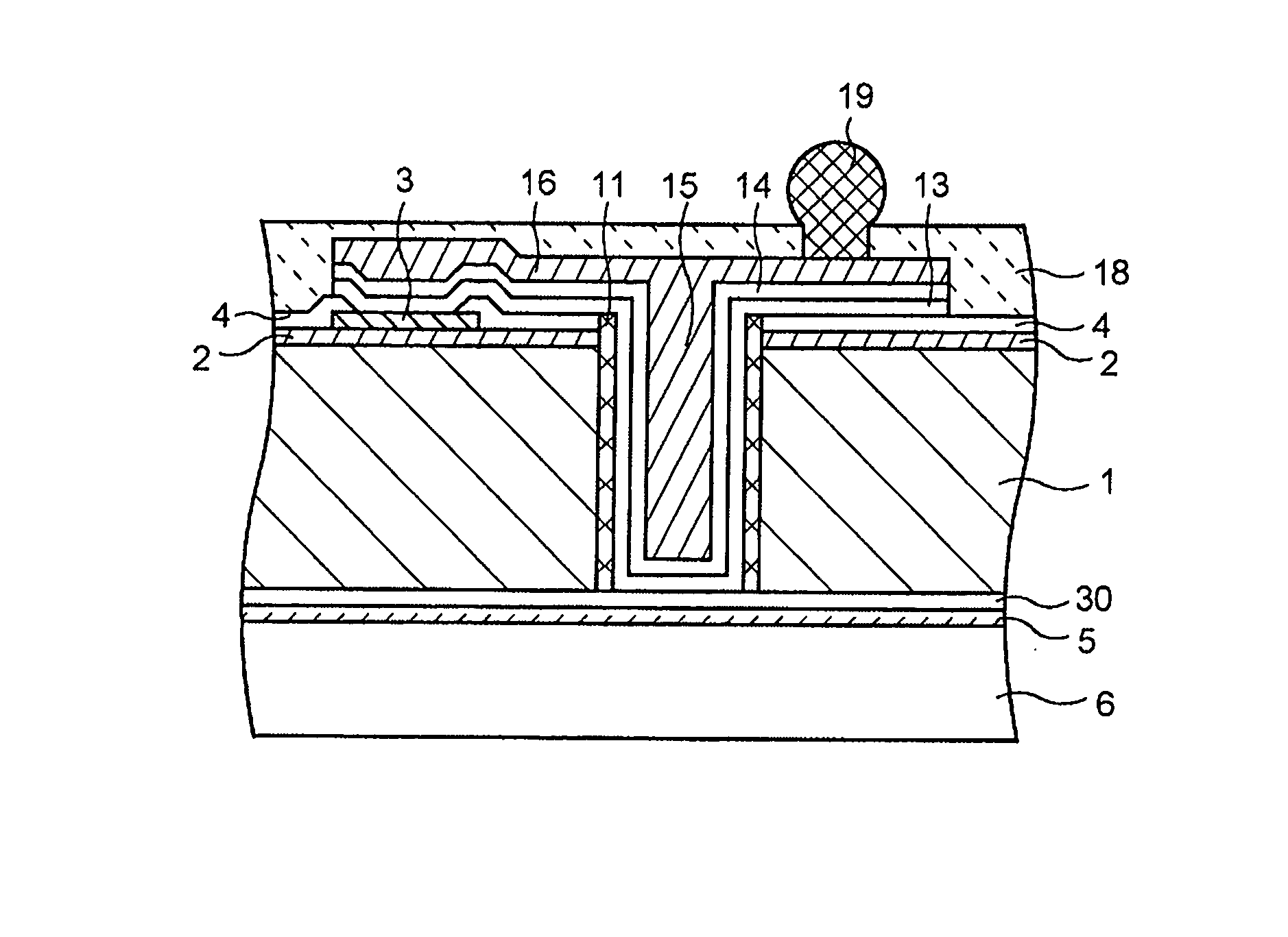
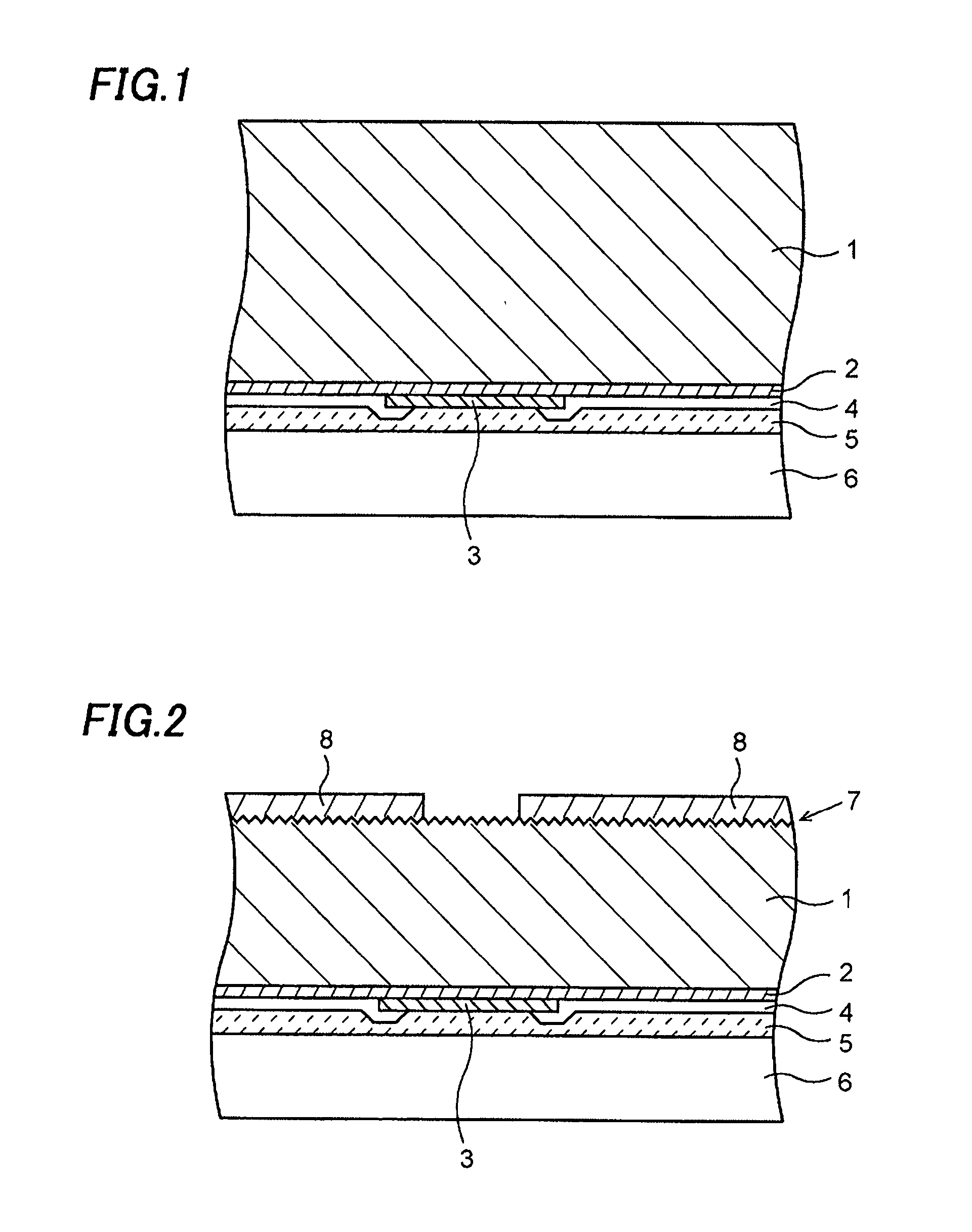
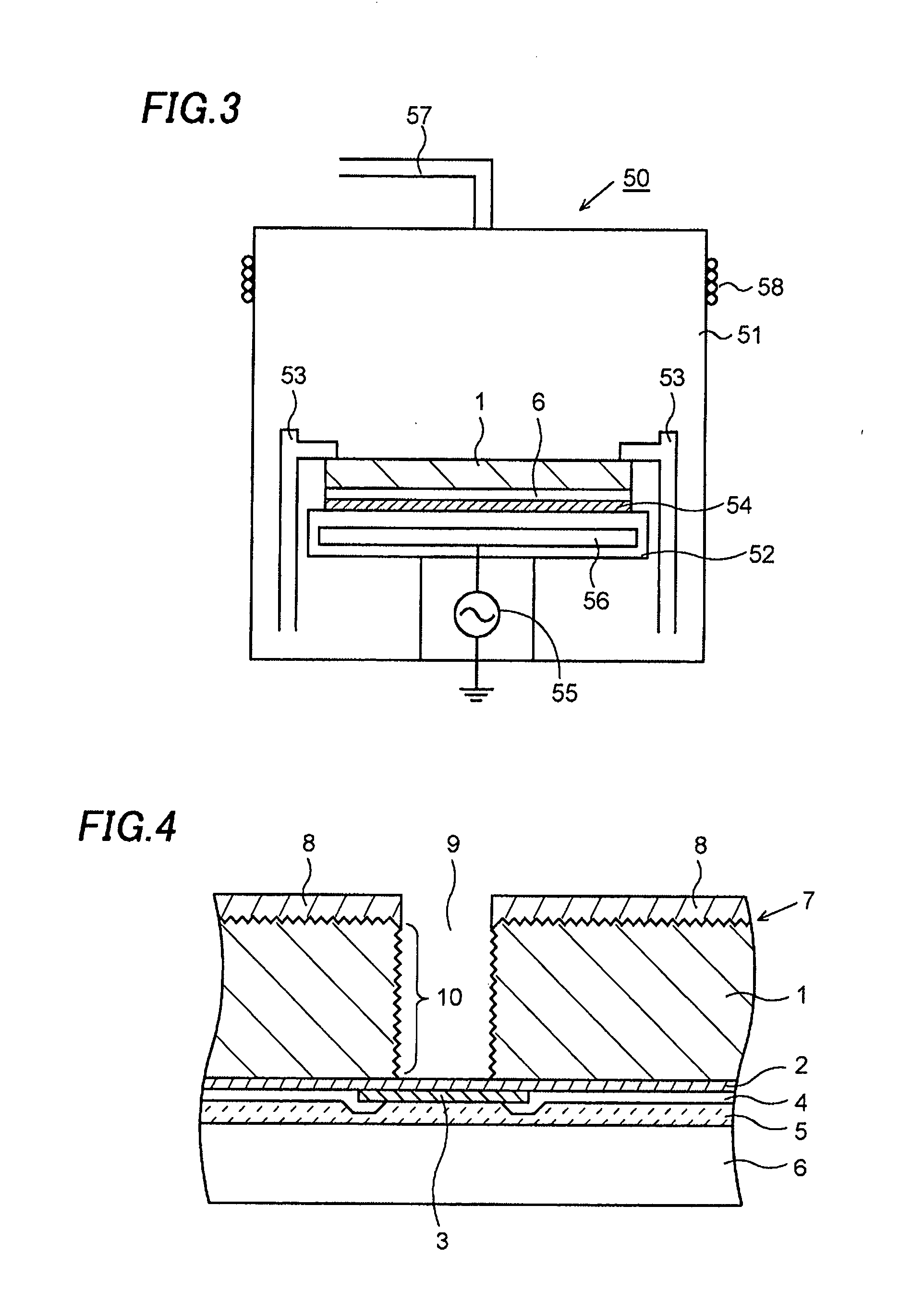
[0028] An embodiment of this invention will be explained hereinafter, referring to the drawings. FIGS. 1 through 10 are cross-sectional views showing a manufacturing method of a semiconductor device according to one embodiment of this invention. Although the manufacturing process is applied to a wafer in which a plurality of the semiconductor devices is arrayed in a matrix bordered with predetermined dicing lines, only one of the semiconductor devices is described hereafter for the simplicity of explanation.

[0029] First, as shown in FIG. 1, there is provided a semiconductor substrate 1, in a front surface of which an electronic device (a CCD, a light-receiving device such as a CCD and an infrared sensor, a light-emitting device or other semiconductor device, for example) is formed. The semiconductor substrate 1 is 8 inches (200 mm) in diameter and 300-700 μm in thickness, for example. A first insulation film 2 (a silicon oxide film or a BPSG (Boro-Phospho Silicate Glass) film forme...


PUM


Abstract

The invention provides a method of manufacturing a semiconductor device which achieves high reliability and high yield as well as high production efficiency. Back surface grinding (back grinding) is performed to a semiconductor substrate to thin the semiconductor substrate. A damaged layer formed by the back surface grinding is not removed at this time, and a photoresist layer is selectively formed on the back surface of the semiconductor substrate. The semiconductor substrate is then etched using the photoresist layer as a mask to form a via hole. The photoresist layer is then removed with the semiconductor substrate still placed in an etcher used in the etching process subsequently after the formation of the via hole. In this manner, the etching process and the next ashing process are performed sequentially in one apparatus. Then a process of removing the damaged layer on the back surface of the semiconductor substrate and a process of smoothing the sidewall of the via hole are simultaneously performed subsequently after the ashing process in the same apparatus.

Description

CROSS-REFERENCE OF THE INVENTION [0001] This invention claims priority from Japanese Patent Application No. 2006-204353, the content of which is incorporated herein by reference in its entirety. BACKGROUND OF THE INVENTION [0002] 1. Field of the Invention [0003] The invention relates to a method of manufacturing a semiconductor device, particularly an etching process and a process of removing a mask layer used in the etching process. [0004] 2. Description of the Related Art [0005] A conventional method of manufacturing a semiconductor device includes an etching process for shaping a foundation insulation film, a metal layer, a semiconductor substrate and the like into a predetermined pattern using a photoresist layer as a mask and an ashing process for removing the photoresist layer used in the etching process. [0006] A description will be given on an example of the conventional method of manufacturing the semiconductor device. As shown in FIG. 13A, back grinding is performed to the...

Claims


Application Information

Patent Timeline
Patent Type & Authority Applications(United States)
IPC IPC(8): H01L21/311H01L21/302H01L23/48
CPCH01L21/3065H01L21/30655H01L21/31138H01L21/76898H01L2224/16H01L2924/09701H01L2924/01046H01L2924/01078H01L2924/01079H01L2924/04941H01L2924/01004H01L24/05H01L2224/02372H01L2224/05008H01L2224/05009H01L2224/05025H01L2224/05147H01L2224/05164H01L2224/05166H01L2224/05181H01L2224/05184H01L2224/05186H01L2224/05548H01L2224/05568H01L2224/05569H01L2224/05644H01L2224/05655H01L2924/00014H01L2924/04953H01L2924/0496H01L2924/01074H01L2924/0494H01L21/02H01L21/302
Inventor SEKI, KATSUYUKISUZUKI, AKIRAKAMEYAMA, KOUJIROOIKAWA, TAKAHIRO
Owner SEMICON COMPONENTS IND LLC
Features
  • Generate Ideas
  • Intellectual Property
  • Life Sciences
  • Materials
  • Tech Scout
  • Unparalleled Data Quality
  • Higher Quality Content
  • 60% Fewer Hallucinations
Learn More