Test Circuit, System, and Method for Testing One or More Circuit Components Arranged upon a Common Printed Circuit Board

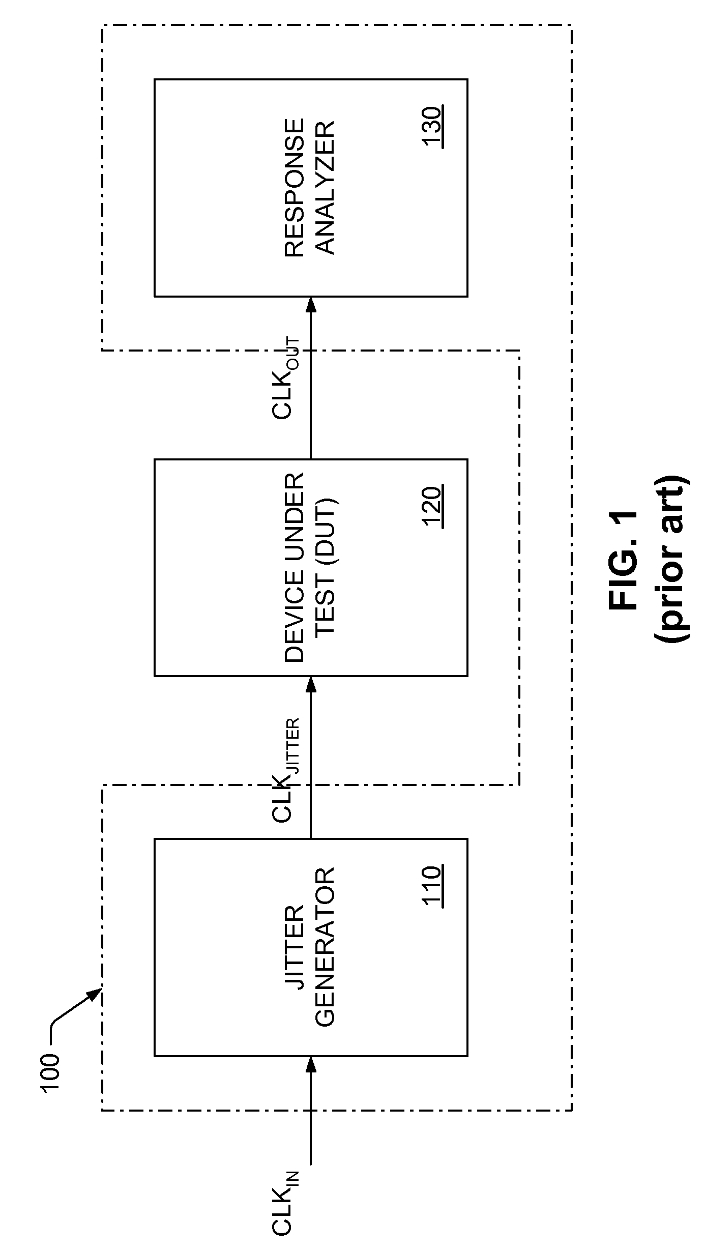
a test circuit and printed circuit technology, applied in the field of integrated circuits, can solve the problems of receiving data signals that are “jittery” relative to the clock signal edges, receiving data signals, and receiving data signals

Inactive Publication Date: 2008-01-31
MONTEREY RES LLC
View PDF28 Cites 30 Cited by
  • Summary
  • Abstract
  • Description
  • Claims
  • Application Information

AI Technical Summary

Benefits of technology

[0025]In some cases, the test circuit may receive and use only one of the plurality of input signals (or one complementary pair of input signals) for generating the test signal. For example, in addition to the jitter generator and output multiplexer, the test circuit may include an input multiplexer, in some embodiments, and one or more additional jitter generators, in other embodiments. In the first embodiment, the input multiplexer may be configured for receiving the plurality of input signals from the clock recovery device and for selecting the one input signal to be supplied to the jitter generator. In the second embodiment, the additional jitter generators may each be configured for receiving a different one of the input signals from the clock recovery device and for generating a dif

Problems solved by technology

Although the transmitter may synchronize the edges (or “signal transitions”) of a digital data signal to the edges of a sample clock signal, variations in signal edge timing (i.e., “jitter”) may cause the receiver to incorrectly sample the received data signal.
For example, noise introduced into the transmitter (or within the clock or data signal paths) may cause the received data signal to appear “jittery” relative to the clock signal edges.
The received data signal may also appear “jittery” to a receiver employing a clock recovery system when feedback errors or noise are introduced therein.
In some cases, jitter may cause the data signal to be shifted sufficiently in time to produce a “bit error” at the receiver when the data signal is incorrectly sampled by the clock signal.
The type of jitter generator used to conduct the jitter tolerance test often impacts the validity of the test results.
Unfortunately, the amplitude of the jitter added to the input signal cannot be controlled in this approach.
Such jitter generators, therefore, cannot be used to measure jitter tolerance.
Thus, one can't measure jitter tolerance without controlling the amplitude of the jitter.
However, in addition to producing uncontrollable ji

Method used


Image

  • Test Circuit, System, and Method for Testing One or More Circuit Components Arranged upon a Common Printed Circuit Board
  • Test Circuit, System, and Method for Testing One or More Circuit Components Arranged upon a Common Printed Circuit Board
  • Test Circuit, System, and Method for Testing One or More Circuit Components Arranged upon a Common Printed Circuit Board

Examples


Embodiment Construction

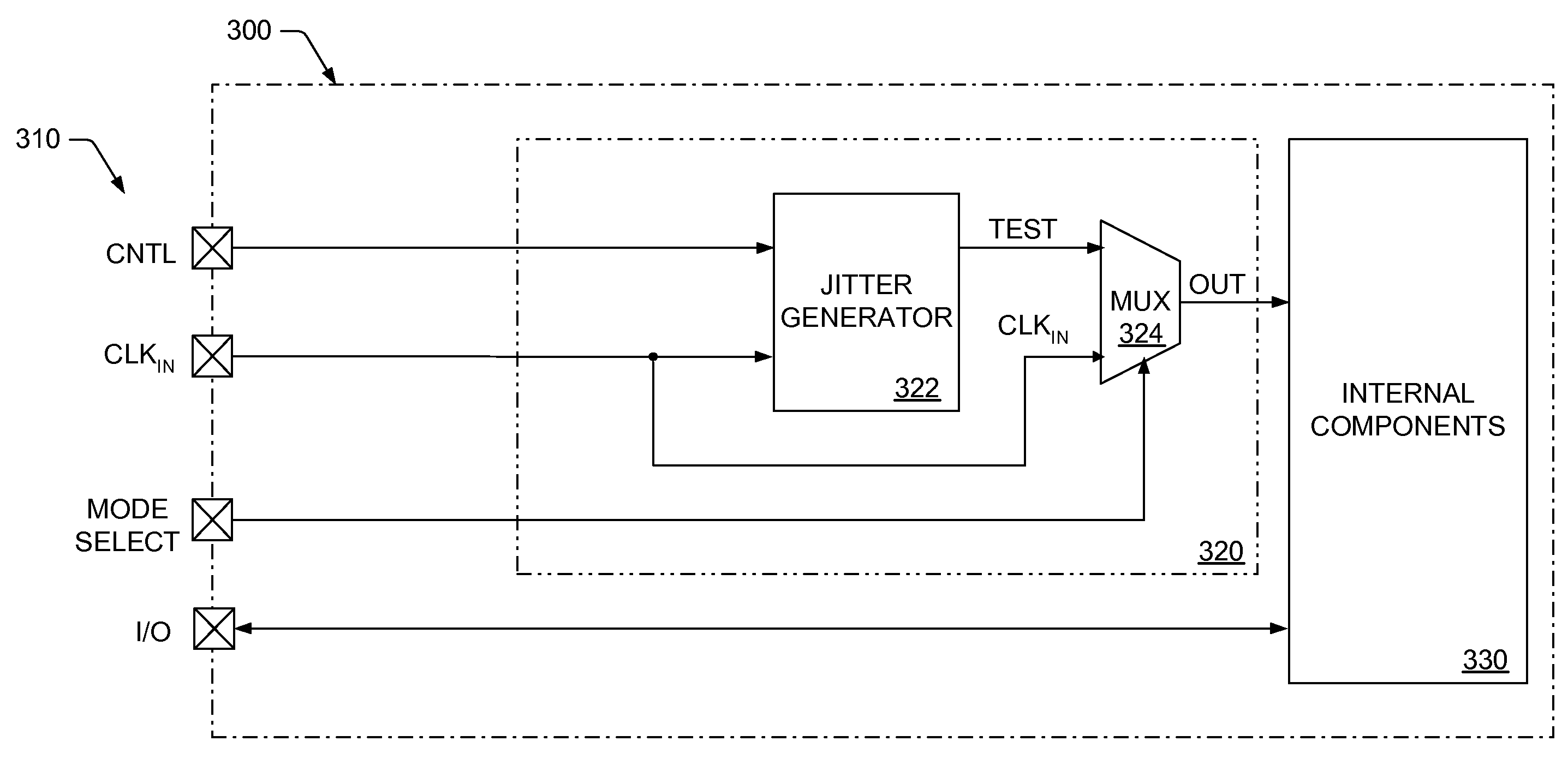
[0041]Exemplary embodiments of a test circuit are shown in FIGS. 3-5. In general, the test circuits described herein may be arranged upon a monolithic integrated circuit (IC) chip or system board (e.g., a printed circuit board) for testing the design margins of any component that may be included within the IC chip or system. For example, the test circuits may be used to determine the jitter and / or duty cycle distortion (DCD) tolerance of an internal component, whose timing is critical to the overall operation of the chip or system. Examples of internal components requiring (or benefiting) from jitter and / or DCD tolerance testing may include, but are not limited to, serial high speed data buses, parallel data buses, and the skew in clock distribution systems. In addition to jitter and DCD tolerance testing, the test circuits described herein may be used to fix design timing margins by changing the clock and data phases.

[0042]Unlike many conventional techniques, the test circuits show...


PUM


Abstract

A test circuit, system, and method are provided herein for testing one or more circuit components arranged upon a monolithic substrate. According to one embodiment, the system may include a test circuit and one or more circuit components, all of which are arranged upon the same monolithic substrate. In general, the test circuit may be configured for: (i) receiving an input signal at an input frequency, (ii) generating a test signal by modulating a phase of the input signal in accordance with a periodic signal, and (iii) supplying either the input signal or the test signal to the one or more integrated circuits, based on a control signal supplied to the test circuit. More specifically, the test circuit may be used to determine the jitter and/or duty cycle distortion (DCD) tolerance of any system component without changing the frequency of the clock signal supplied to the component or injecting noise into the clock recovery system.

Description

BACKGROUND OF THE INVENTION[0001]1. Field of the Invention[0002]This invention relates to integrated circuits (ICs) and, more particularly, to an internal test circuit that may be used for supplying a highly controlled amount of jitter and / or duty cycle distortion to one or more circuit components arranged upon a common printed circuit board.[0003]2. Description of the Related Art[0004]The following descriptions and examples are given as background only.[0005]Many electronic systems (such as communication systems, computer systems, etc.) communicate by transmitting digital data signals between transmitting and receiving portions of the system. To avoid errors, the system receiver must sample the received data signal at the same frequency and phase with which the signal was initially digitized by the system transmitter.[0006]In some cases, the transmitter may send a clock signal along with the digital data signal for controlling the timing with which the receiver samples the digital ...

Claims


Application Information

Patent Timeline
IPC IPC(8): H04B3/46
CPCG01R31/31709G01R31/31937G01R31/31922
Inventor LI, GABRIEL
Owner MONTEREY RES LLC
Why Eureka
Try Eureka