
Wired circuit board

Inactive Publication Date: 2008-02-07
NITTO DENKO CORP
View PDF12 Cites 17 Cited by
  • Summary
  • Abstract
  • Description
  • Claims
  • Application Information

AI Technical Summary

Benefits of technology

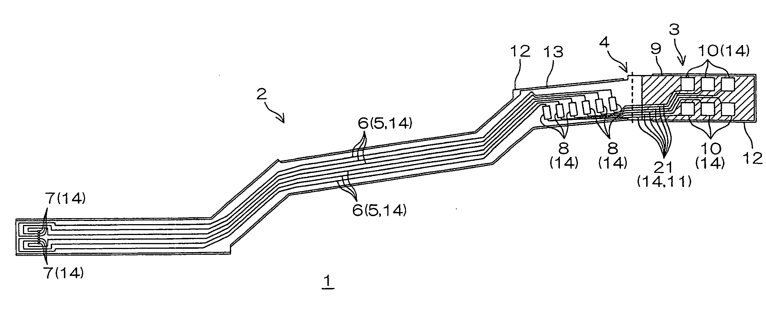
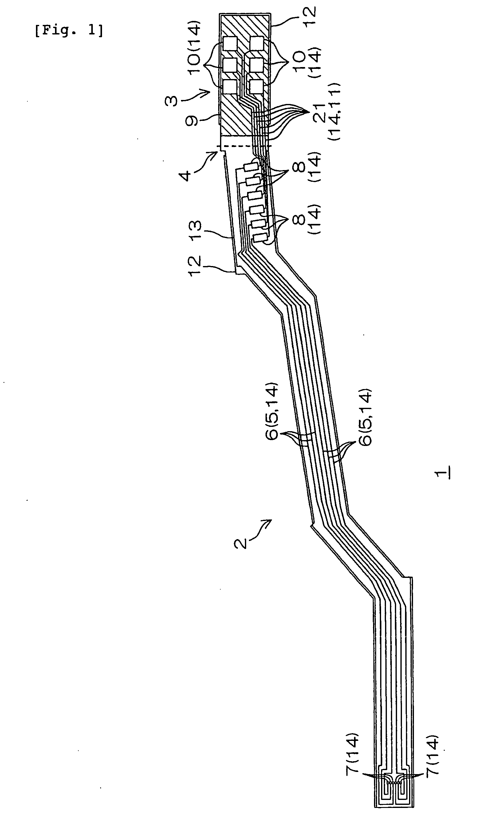
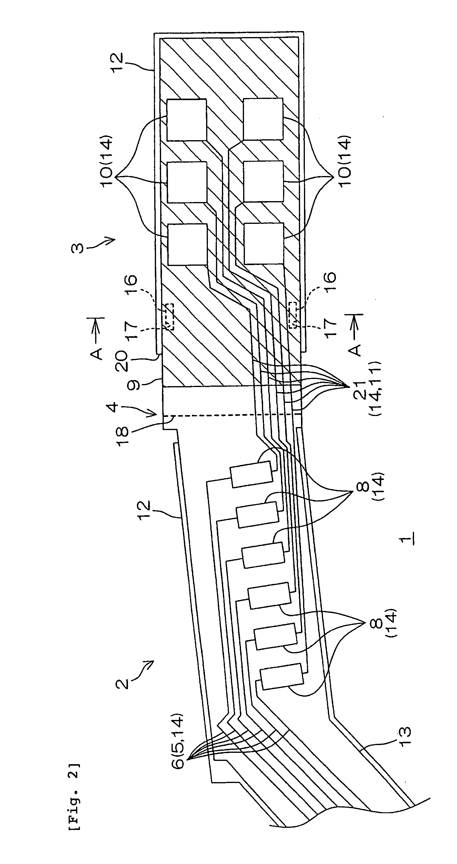
[0037]According to this wired circuit board, before an electronic component is mounted on the wired circuit body portion, static electricity charged thereon can be efficiently removed via the semiconductive layer of the electrostatic charge removing portion that is conducted with the wired circuit body portion.
[0038]After an electronic component is mounted on the wired circuit body portion, electrical conduction between the wired circuit body portion and the electrostatic charge removing portion is already cut off by the conduction cut-off portion, so that it is possible to prevent the wired circuit of the wired circuit body portion from being electrically affected by the semiconductive layer of the electrostatic charge removing portion. Accordingly, the electrical stability of the wired circuit body portion can be reliably secured.

Problems solved by technology

In contrast to this, after an electronic component is mounted thereon, there is a possibility that the semiconductive layer may impair the electrical stability of the wired circuit board during energization.
As a result, there is a possibility that as described above, the semiconductor layer may impair the electrical stability and long term reliability of the suspension board with circuit during energization.

Method used


Image

  • Wired circuit board
  • Wired circuit board
  • Wired circuit board

Examples


example 1

[0209]A metal supporting layer of a stainless foil having a thickness of 20 μm was prepared (cf. FIG. 4(a)).

[0210]Subsequently, a varnish of photosensitive polyamic acid resin was uniformly coated over a surface of the metal supporting layer using a spin coater. The coated varnish was then heated at 90° C. for 15 minutes to form a base coating. Thereafter, the base coating was exposed to light at 700 mJ / cm2 via a photomask, and then heated at 190° C. for 10 minutes. The base coating thus heated was developed using an alkaline developer. Subsequently, the coating was cured at 385° C. under the pressure reduced to 1.33 Pa, thereby forming an insulating base layer of polyimide on the metal supporting layer to correspond to a portion where a conductive pattern was formed, and to provide the above-mentioned pattern in which base openings are formed (cf. FIG. 4(b)). The insulating base layer thus formed had a thickness of 10 μm. Each of the base openings had a rectangular shape in plane v...


PUM


Abstract

[Object] To provide a wired circuit board in which charged static electricity can be efficiently removed before mounting of electronic components and electrical stability of a wired circuit body portion can be reliably secured after the mounting of the electronic components.[Solution Means] In a suspension board with circuit 1 in which a metal supporting layer 12, an insulating base layer 13, a conductive pattern 14 having a main wired circuit 5 formed on a wired circuit body portion 2 and an auxiliary wired circuit 11 formed on an electrostatic charge removing portion 3, and an insulating cover layer 15 are sequentially laminated, a semiconductive layer 9 covering the auxiliary wired circuit 11 is formed on the insulating base layer 13 in the electrostatic charge removing portion 3. Before mounting of a magnetic head, static electricity charged on the wired circuit body portion 2 can be efficiently removed via the semiconductive layer 9. After the mounting of the magnetic head, the electrostatic charge removing portion 3 is separated from the wired circuit body portion 2 using a conduction cut-off portion 4 as a boundary, so that electrical conduction between the wired circuit body portion 2 and the electrostatic charge removing portion 3 is cut off.

Description

TECHNICAL FIELD[0001]The present invention relates to a wired circuit board. More particularly, the present invention relates to a wired circuit board for mounting an electronic component, such as a suspension board with circuit.PRIOR ART[0002]A wired circuit board such as a suspension board with circuit includes, for example, a metal supporting board of stainless steel foil or the like, an insulating base layer of polyimide resin or the like, which is formed on the metal supporting board, a conductive pattern of copper foil or the like, which is formed on the insulating base layer, and an insulating cover layer of polyimide resin or the like, which is formed on the insulating base layer to cover the conductive pattern. The wired circuit boards of this type are widely used in a variety of fields of electric and electronic equipment.[0003]In such wired circuit board, in order to prevent electronic components mounted thereon from electrostatic breakdown, there has been proposed that a...

Claims


Application Information

Patent Timeline
IPC IPC(8): H05K1/00
CPCG11B5/486G11B5/6094H05K1/0259H05K1/056H05K2201/0969H05K3/28H05K2201/09063H05K2201/09554H05K1/167
Inventor OOYABU, YASUNARIISHII, JUNTERADA, NAOHIRO
Owner NITTO DENKO CORP
Learn More