Display apparatus and electronic device

a technology of electronic devices and display devices, applied in the direction of instruments, static indicating devices, etc., can solve the problems of difficult application to large and high-definition displays, and achieve the effects of increasing brightness, increasing the amount of drive current flowing through the switching transistor and the drive transistor, and increasing the brightness

Inactive Publication Date: 2008-02-07
THOMSON LICENSING SA
View PDF4 Cites 10 Cited by
  • Summary
  • Abstract
  • Description
  • Claims
  • Application Information

AI Technical Summary

Benefits of technology

[0020] With the present invention, the sizes of the switching transistor and the drive transistor are devised in such a manner that the mobility corrective function operates appropriately. In other words, the size of the switching transistor is made larger than the size of the drive transistor so that the on resistance of the switching transistor would be lower than the on resistance of the drive transistor. As described above, with the present invention, mobility correction is performed by negatively feeding back to the pixel capacitance the drive current flowing from the drive transistor. In so doing, the amount of negative feedback increases as the signal potential becomes higher (and therefore the brightness greater). In other words, when the brightness is high, the amount of drive current flowing through the switching transistor and the drive transistor becomes greater. Therefore, as the brightness becomes higher, variations in the on resistance of the switching transistors become more pronounced. As such, effects of variations in the on resistance of the switching transistor at high-brightness side appear even though variations in the mobility of the drive transistor (in other words, variations in the on resistance of the drive transistor) are corrected for, and uniformity of the screen would thus be compromised. As such, by reducing the on resistance of the switching transistor to, preferably, a quarter or below of the on resistance of the drive transistor, effects on the amount of negative feedback are suppressed. With such a configuration, such image degradation as uneven streaks that are caused by variations in the on resistance of the switching transistors at high brightness scales is resolved, and it is thus possible to further improve uniformity.

Problems solved by technology

While the former has a simple structure, it has a problem in that application to large and high definition displays is difficult.

Method used


Image

  • Display apparatus and electronic device
  • Display apparatus and electronic device
  • Display apparatus and electronic device

Examples


Embodiment Construction

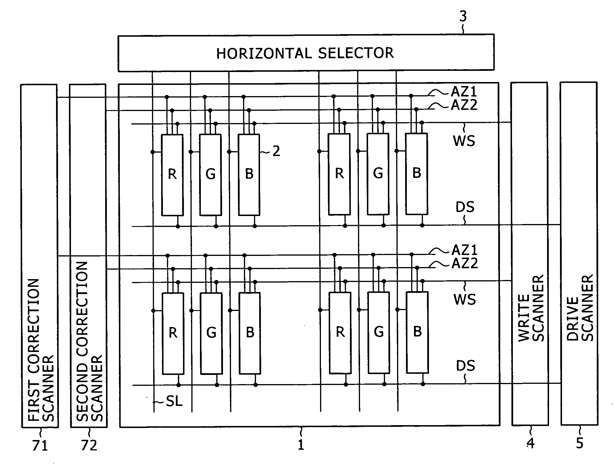
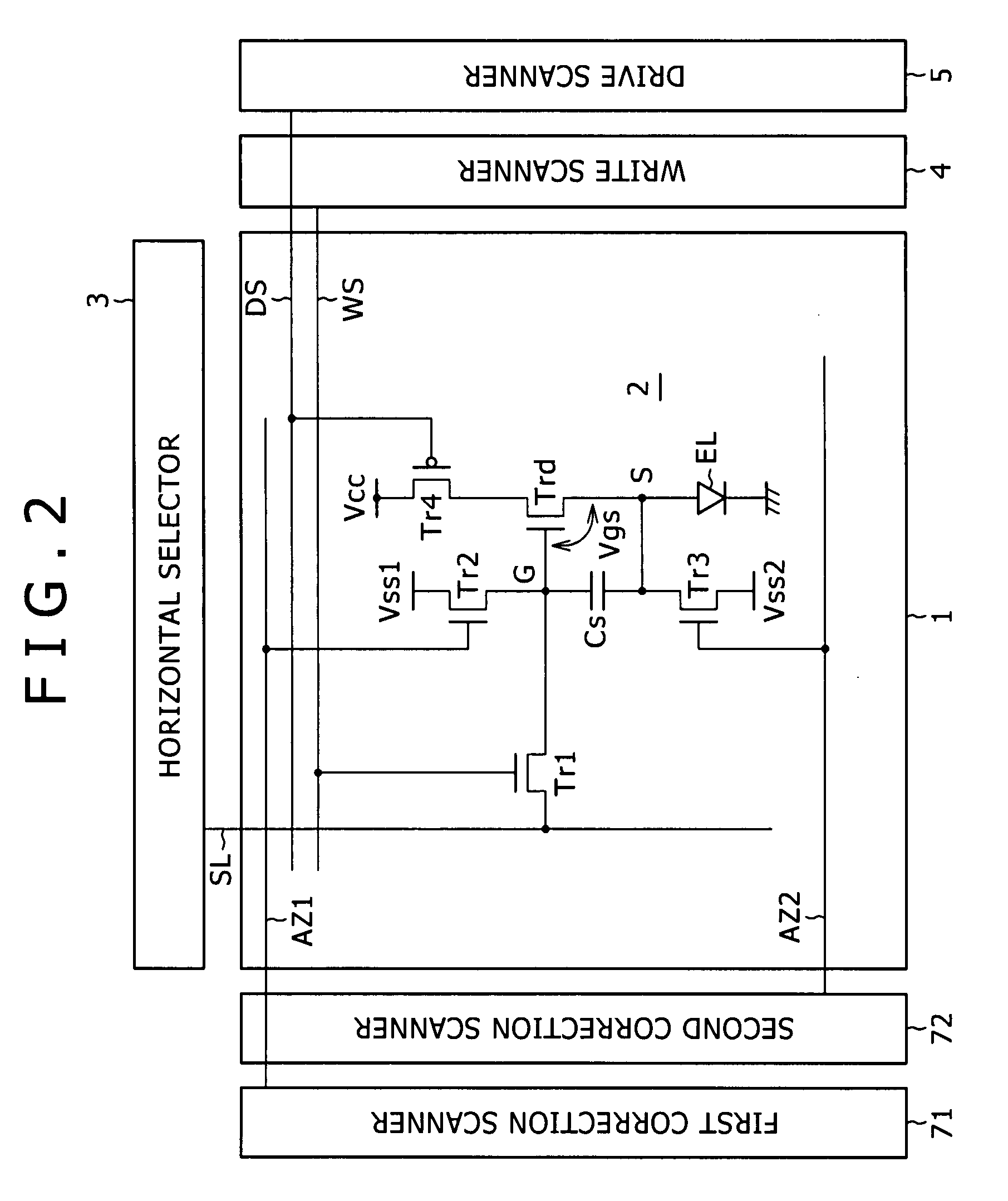
[0035] Embodiments of the present invention are described in detail with reference to the drawings. FIG. 1 is a schematic block diagram indicating the overall configuration of a display apparatus according to an embodiment of the present invention. In this diagram, the image display apparatus basically includes a pixel array section 1, and a drive section that includes a scanner section and a signal section. The pixel array section 1 includes scanning lines WS, AZ1, AZ2 and DS that are arranged in rows, signal lines SL that are arranged in columns, and matrix pixel circuits 2, which are connected to these scanning lines WS, AZ1, AZ2 and DS, and the signal lines SL, and a plurality of power lines which supply a first potential Vss1, a second potential Vss2, and a third potential Vcc which are necessary for operation of each of the pixel circuits 2. The signal section includes a horizontal selector 3, and supplies video signals to the signal lines SL. The scanner section includes a li...


PUM


Abstract

A display apparatus, comprising a pixel array section and a drive section that drives the pixel array section, wherein the pixel array section includes first scanning lines and second scanning lines arranged in rows, signals lines arranged in columns, matrix pixels that are provided where the first scanning lines, the second scanning lines, and the signal lines cross, and a power line that supplies power to each of the pixels, and an earth line. The drive section includes a first scanner that sequentially line scans the pixels in rows by sequentially supplying a first control signal to each of the first scanning lines, a second scanner that sequentially supplies a second control signal to each of the second scanning lines in conjunction with the sequential line scanning, and a signal selector that supplies video signals to the columns of signal lines in conjunction with the sequential line scanning.

Description

BACKGROUND OF THE INVENTION [0001] 1. Field of the Invention [0002] The present invention relates to a display apparatus that displays images by driving light emitting elements arranged by pixels by an electric current. More specifically, the present invention relates to a display apparatus of the so-called active matrix type in which the amount of current that is passed through a light emitting element, such as an organic EL element and the like, is controlled by an insulated gate type field effect transistor that is provided in each pixel circuit. More specifically, the present invention relates to a technology for optimizing the size of the transistor that is formed in each of the pixel circuits, and it also relates to an electronic device into which such a display apparatus is incorporated. [0003] 2. Description of Related Art [0004] In image displaying apparatuses, such as liquid crystal displays, for example, numerous liquid crystal pixels are arranged in a matrix, and an imag...

Claims


Application Information

Patent Timeline
Patent Type & Authority Applications(United States)
IPC IPC(8): G09G3/32
CPCG09G3/3233G09G2300/0417G09G2300/043G09G2320/043G09G2300/0842G09G2310/0256G09G2320/0233G09G2300/0819
Inventor UCHINO, KATSUHIDEYAMASHITA, JUNICHITOYOMURA, NAOBUMI
Owner THOMSON LICENSING SA
Why Eureka
Try Eureka