

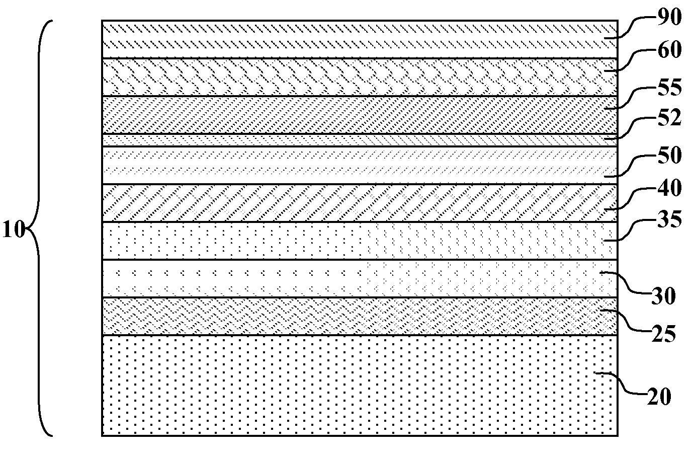
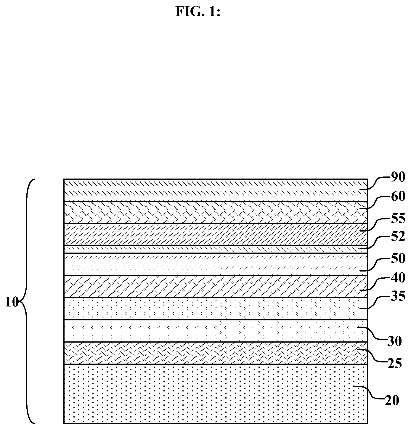
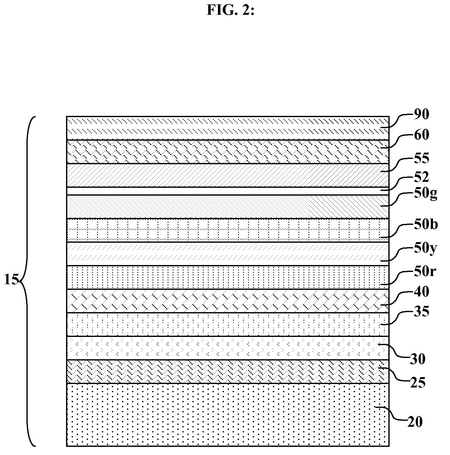
Dual electron-transporting layer for OLED device
a technology of electron transporting layer and oled device, which is applied in the field of white oled device, can solve the problems of device not having all desired el characteristics in terms of high luminance, device performance limitations that have represented a barrier to many desirable applications, and inferior stability of bphen/alq mix of seo et al., etc., and achieves the effect of reducing the voltage requirements of an oled device and improving efficiency and stability
- Summary
- Abstract
- Description
- Claims
- Application Information
AI Technical Summary
Benefits of technology
Problems solved by technology
Method used
Image

Examples
example 4 (
INVENTIVE)
[0119]An inventive color OLED display was constructed as in Example 3, except that Step 7 was as follows:[0120]7. A 3 nm mixed electron-transporting layer was vacuum-deposited, including 1.5 nm BNA and 1.5 nm LiQ.
example 5 (
INVENTIVE)
[0121]An inventive color OLED display was constructed as in Example 3, except that Step 7 was as follows:[0122]7. A 3 nm layer of BNA was vacuum-deposited.
[0123]The results of testing these examples are shown in Table 1, below. Example 1 shows the results for an OLED device known in the art. Example 2 demonstrates the addition of dopant lithium to the electron-transporting layer, with a strong decrease in luminance efficiency and fade stability. The addition of a thin lithium-free electron-transporting layer comprising lithium quinolate between the standard electron-transporting layer and the emitting layers, as in Example 3, gives improved luminance efficiency and lower drive voltage, but the fade stability is still poor. However, the use of an anthracene in the thin electron-transporting layer, as in Examples 4 and 5, gives good stability while retaining good drive voltage and luminance efficiency.
TABLE 1Device data measured at 20 mA / cm2 (except as noted)Room TempFade St...
PUM
 Abstract
Description
Claims
Application Information