
Eureka
For R&D, Eureka makes reading and utilizing patents & technical documents easy.
Eureka AIR
Designed for self-driven R&D workflows. Generate viable solutions, solve complex R&D challenges, empower your innovation with AI.

Eureka Materials
Designed for material experts only. Revolutionize your material R&D, from search, analyze, to developing new materials.

TechResearch
Generate reliable direction feasibility study reports for your R&D in just a few steps.

TechSeek
Discover and master advanced knowledge NOW. Basics, ideas, possibilities, all at once.

TechMind
As an expert in R&D Theories, TechMind can generates customized viable solutions instantly.

TechRisk
Analyze your overall solution with one click, know your potential R&D risks in advance.

TechMonitor
Get weekly tech updates, stay abreast of the latest tech innovations and key insights.
Semiconductor device and method of fabricating semiconductor device
- Summary
- Abstract
- Description
- Claims
- Application Information
AI Technical Summary
Benefits of technology
Problems solved by technology
Method used
Image

Examples
first exemplary embodiment
[0030]First, a first exemplary embodiment in accordance with the present invention will be described in detail by using the drawings.
(Structure)
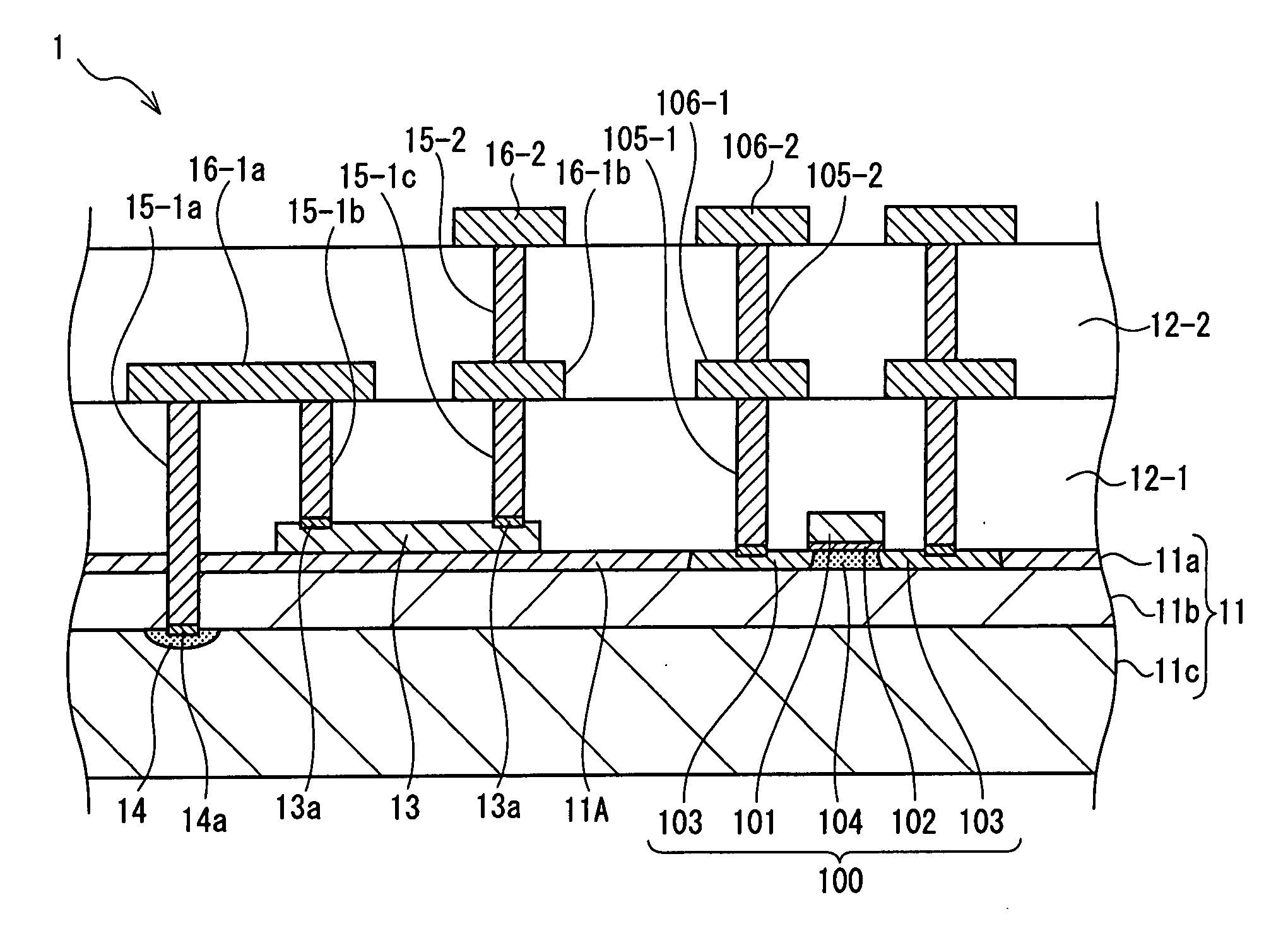
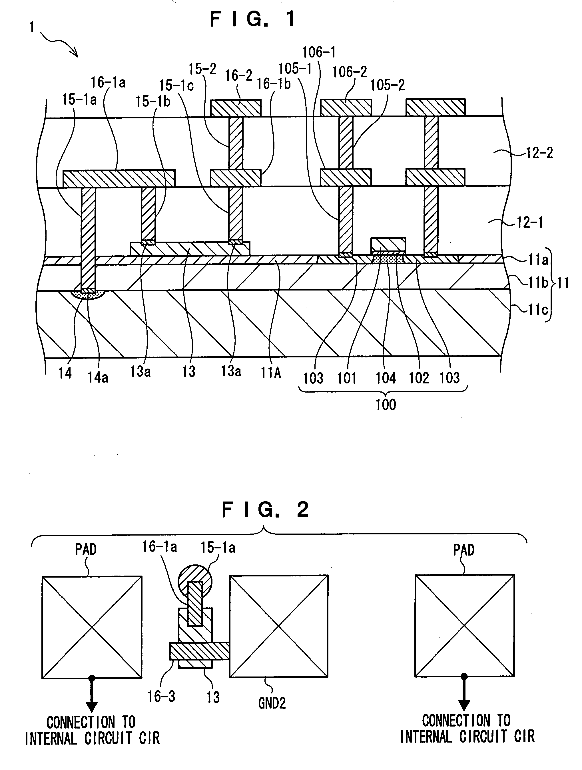
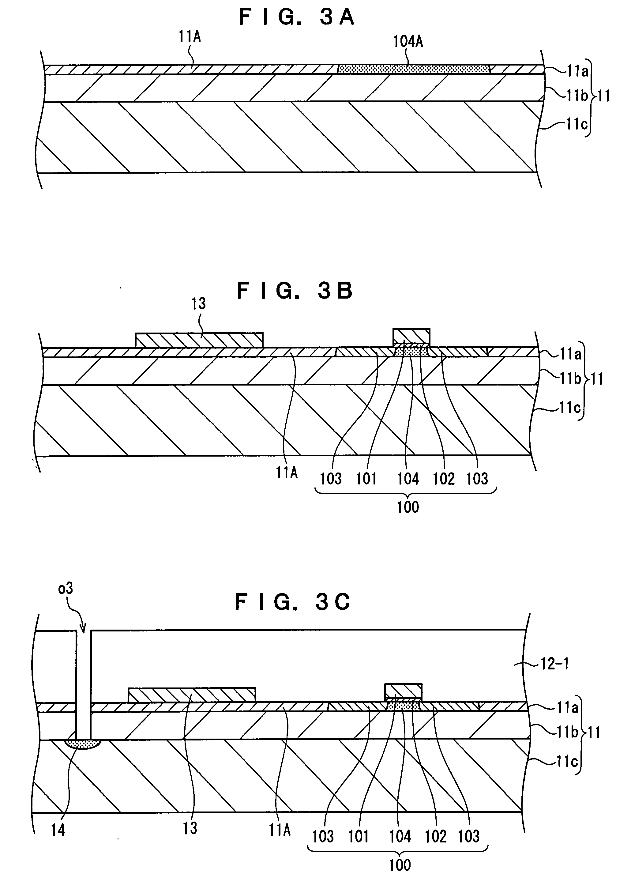
[0031]FIG. 1 is a cross-sectional view showing a layer structure of a semiconductor device 1 in accordance with the present exemplary embodiment. As shown in FIG. 1, the semiconductor device 1 has an SOI substrate 11, interlayer insulating films 12-1 and 12-2, a resistance element 13, a substrate contact 15-1a, via wires 15-1b through 15-2, lowermost layer metal wires 16-1a and 16-1b, an upper layer metal wire 16-2, a transistor 100, via wires 105-1 and 105-2, lowermost layer metal wires 106-1, and upper layer metal wires 106-2.
[0032]In this structure, the SOI substrate 11 has a supporting substrate 11c, a BOX layer 11b, and an SOI layer 11a.
[0033]The supporting substrate 11c is a bulk silicon substrate which is doped such that, for example, the p-type impurities are a concentration of about 1×10¹⁵ / cm3 for example. The substrate resistance ...
second exemplary embodiment
[0066]A second exemplary embodiment of the present invention will be described in detail next by using the drawings. Note that, in the following explanation, structures which are similar to those of the first exemplary embodiment are denoted by the same reference numerals, and detailed description thereof is omitted. Further, structures which are not mentioned specially are similar to those of the first exemplary embodiment.
(Structure)
[0067]FIG. 6 is a cross-sectional view showing the layer structure of a semiconductor device 2 in accordance with the present exemplary embodiment. As shown in FIG. 6, the semiconductor device 2 has a structure in which, in a structure similar to the semiconductor device 1 of the first exemplary embodiment, the resistance element 13 is replaced by a depression-type MOS transistor (hereinafter, DMOS transistor) 20. Note that, because the other structures are similar to those of the semiconductor device 1 in accordance with the first exemplary embodiment...
third exemplary embodiment
[0082]A third exemplary embodiment of the present invention will be described in detail next by using the drawings. Note that, in the following explanation, structures which are similar to those of the first exemplary embodiment or the second exemplary embodiment are denoted by the same reference numerals, and detailed description thereof is omitted. Further, structures which are not mentioned specially are similar to those of the first exemplary embodiment or the second exemplary embodiment.
[0083]The present exemplary embodiment describes, as an example, a case in which a wire is formed which electrically connects the substrate contact 15-1a and the ground end of the semiconductor element (the transistor 100 in the present explanation). Note that, when describing the present exemplary embodiment hereinafter, structures of the semiconductor device 1 in accordance with the first exemplary embodiment are cited. However, the present invention is not limited to the same, and can similar...
PUM
 Abstract
Description
Claims
Application Information
 - R&D Engineer
- R&D Manager
- IP Professional
- Industry Leading Data Capabilities
- Powerful AI technology
- Patent DNA Extraction
Browse by: Latest US Patents, China's latest patents, Technical Efficacy Thesaurus, Application Domain, Technology Topic, Popular Technical Reports.
© 2024 PatSnap. All rights reserved.Legal|Privacy policy|Modern Slavery Act Transparency Statement|Sitemap|About US| Contact US: help@patsnap.com