Semiconductor device and method for manufacturing the same

a semiconductor device and manufacturing method technology, applied in the field of semiconductor devices and semiconductor device manufacturing methods, can solve the problems of deterioration in reliability of electrical characteristics of phase-change memory, thinned portion of the upper electrode film is susceptible to etching damage, and may be buried at the bottom of the via hole, so as to improve the reliability of semiconductor devices

Inactive Publication Date: 2007-02-08
RENESAS TECH CORP
View PDF2 Cites 99 Cited by
  • Summary
  • Abstract
  • Description
  • Claims
  • Application Information

AI Technical Summary

Benefits of technology

[0015] An object of the present invention is to provide a techn

Problems solved by technology

However, when the via hole for forming the plug is formed on the upper electrode film, the upper electrode film may be thinned at the bottom of the via hole due to over-etching.
Moreover, the thinned portion of the upper electrode film is susceptible to etching damage at the time of dry etching and heat-load damage at the time of forming a conductive film for plug.
This will cause deterioration in reliability of electrical characteristics of the phase-change memory.
Also, when the via hole for forming the plug is formed on the upper electrode film, the occurrence of misalignment (alignment deviation) may cause a sidewall of the recording layer (phase-change film) to be exposed from the via hole.
The recordin

Method used


Image

  • Semiconductor device and method for manufacturing the same
  • Semiconductor device and method for manufacturing the same
  • Semiconductor device and method for manufacturing the same

Examples


first embodiment

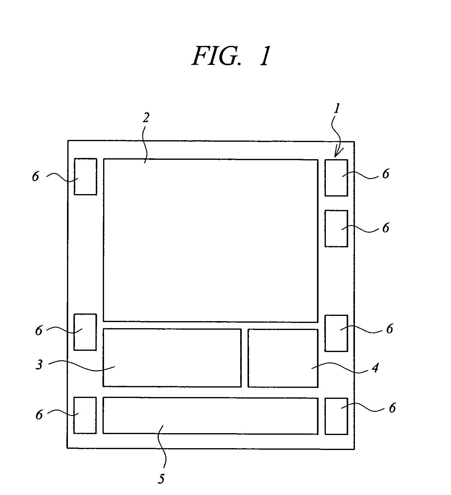
[0090] A semiconductor device and semiconductor device manufacturing method according to a first embodiment is described with reference to drawings. FIG. 1 is a plan view (plan layout or chip layout) of a schematic structure of a semiconductor device (non-volatile semiconductor storage device or semiconductor chip) according to the first embodiment of the present invention;

[0091] A semiconductor device (semiconductor chip) 1 according to the present invention is a semiconductor device (semiconductor storage device) including a phase-change memory (phase-change non-volatile memory, PCM (Phase Change Memory), OUM (Ovonic Unified Memory)), which is a phase-change non-volatile memory (non-volatile storage element).

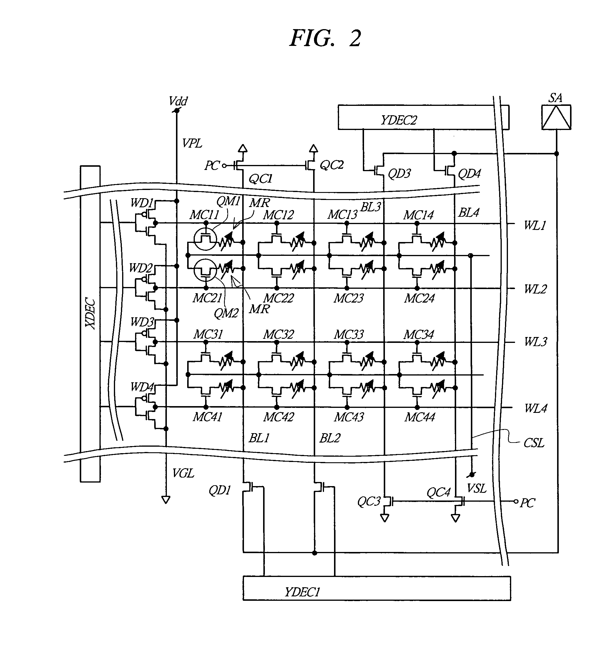
[0092] As shown in FIG. 1, the semiconductor device 1 according to the present invention has a phase-change memory area 2 having formed therein a memory cell array of phase-change memory. Furthermore, the semiconductor device 1 includes, as required, a RAM area 3 having form...

second embodiment

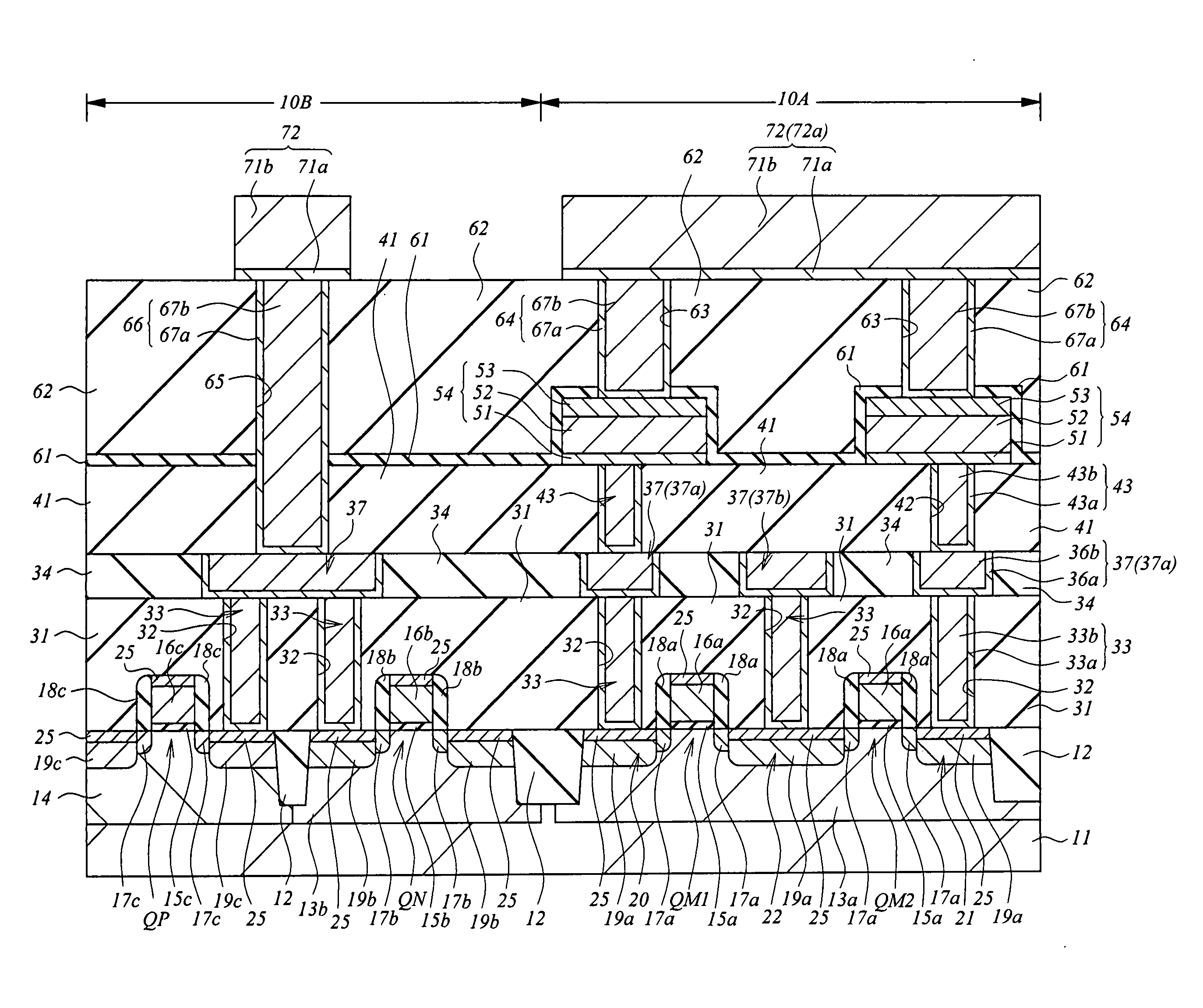
[0208] In the first embodiment described above, the upper electrode film 53 and the recording layer 52 are patterned to form the resistor element 54, and then the insulation film 61 as an etching stopper film is formed so as to cover the resistor element 54. In the present embodiment, an insulation film 61a as an etching stopper film is formed before the recording layer 52 and the upper electrode film 53 are patterned.

[0209] FIGS. 35 to 40 are cross-section views of main parts of a semiconductor device according to the present embodiment during the manufacturing process continued from FIG. 15 of the first embodiment. The manufacturing process up to FIG. 15 is similar to that of the first embodiment, and therefore is not described herein, and the process continued from FIG. 15 is now described. Here, for ease of understanding, in FIGS. 35 to 40, like in FIGS. 15 to 22 of the first embodiment, the insulation film 31 and portions corresponding to the structure therebelow in FIG. 14 ar...

third embodiment

[0220] In the first and second embodiments, the resistor element 54 is separated in a bit. In the present embodiment, the phase-change memory cell structure is such that the resistor element 54 is successively provided in a bit.

[0221]FIGS. 41 and 42 are cross-section views of main parts of a semiconductor device according to the present embodiment during the manufacturing process continued from FIG. 35 of the second embodiment. The manufacturing process up to FIG. 35 is similar to that of the second embodiment, and therefore is not described herein, and the process continued from FIG. 35 is now described. Here, for ease of understanding, in FIGS. 41 and 42, like in FIGS. 15 to 22 of the first embodiment, the insulation film 31 and portions corresponding to the structure therebelow in FIG. 14 are omitted.

[0222] After the structure shown in FIG. 35 is formed in a manner similar to that of the second embodiment, as shown in FIG. 41, with a photoresist pattern (not shown) formed on th...


PUM


Abstract

A resistor element formed of a peel-preventive film, a recording layer made of chalcogenide, and an upper electrode film is formed on a semiconductor substrate, first and second insulation films are formed so as to cover the resistor element, a via hole for exposing the upper electrode film is formed through the first and second insulation films, and a plug for electrical connection to the upper electrode film is formed in the via hole. To form the via hole, the first insulation film made of silicon nitride is used as an etching stopper to perform dry etching on the second insulation film. Then, dry etching is performed on the first insulation film to expose the upper electrode film from the via hole.

Description

CROSS-REFERENCE TO RELATED APPLICATION [0001] The present application claims priority from Japanese Patent Application No. JP 2005-224389 filed on Aug. 2, 2005, the content of which is hereby incorporated by reference into this application. TECHNICAL FIELD OF THE INVENTION [0002] The present invention relates to semiconductor devices and semiconductor device manufacturing methods and, particularly, to a technology effective when applied to a semiconductor device including a phase-change memory and a method of manufacturing such a semiconductor device. BACKGROUND OF THE INVENTION [0003] In a non-volatile semiconductor storage device for data storage, various schemes for storing data in a memory cell can be adopted. In one scheme, a phase-change memory is utilized, which is a non-volatile memory using a phase-change film. [0004] The phase-change memory is a non-volatile memory in which information to be stored is written, with a crystalline state of a storage element being changed in ...

Claims


Application Information

Patent Timeline
IPC IPC(8): H01L23/52
CPCG11C13/0004G11C13/0069G11C2013/0078G11C2213/79H01L45/06H01L27/2463H01L45/1233H01L45/144H01L45/1675H01L27/2436H01L45/12H10B63/30H10B63/80H10N70/801H10N70/231H10N70/826H10N70/8828H10N70/063
Inventor TAKAURA, NORIKATSUMATSUZAKI, NOZOMU
Owner RENESAS TECH CORP
Why Eureka
Try Eureka