RFID tag and method for reading the same

a technology of rfid tags and rfid tags, which is applied in the field of rfid (radio frequency identification) tags, can solve the problems of rfid tags coming off by mistake, and it is fairly difficult to place laminated rfid tags through the intermediary of the first spacer in a narrow clearance between the surface of the metal case and the resin container, so as to reduce the variation in the quality of rfid tag products, and the effect of downsiz

Inactive Publication Date: 2008-02-14
HITACHI LTD
View PDF9 Cites 37 Cited by
  • Summary
  • Abstract
  • Description
  • Claims
  • Application Information

AI Technical Summary

Benefits of technology

[0012]According to an aspect of an RFID tag and a method for reading the RFID tag of the present invention, compared to the second antenna that resonates at a communication frequency, the length of the first antenna which has an IC chip and which is magnetically coupled to the second antenna is made shorter, so that even if some displacement occurs in the relative position of the first and second antennas, changes are less likely to occur in the characteristics, such as resonance frequency and gain, thus reducing variations in quality of RFID tag products.
[0013]According to another aspect of the RFID tag and the method for reading the RFID tag of the present invention, in addition to the above-mentioned effects, because the resin container is used as the second spacer, the implementation clearance can be made smaller, which contributes to down-sizing of an electronic device to which the present invention is applied.
[0014]According to a yet additional aspec

Problems solved by technology

Therefore, manufactured individual IC tags for wireless use have variations in performance, which has been a difficult problem.
There is another problem that to lengthen the communication distance, it is necessary to provide a long separation distance between the first antenna and the second antenna, and accordingly some implementation space (mounting space) has to be provided.
In an electronic device structured as described, if a conventional multilayered RFID tag is mounted

Method used


Image

  • RFID tag and method for reading the same
  • RFID tag and method for reading the same
  • RFID tag and method for reading the same

Examples


first embodiment

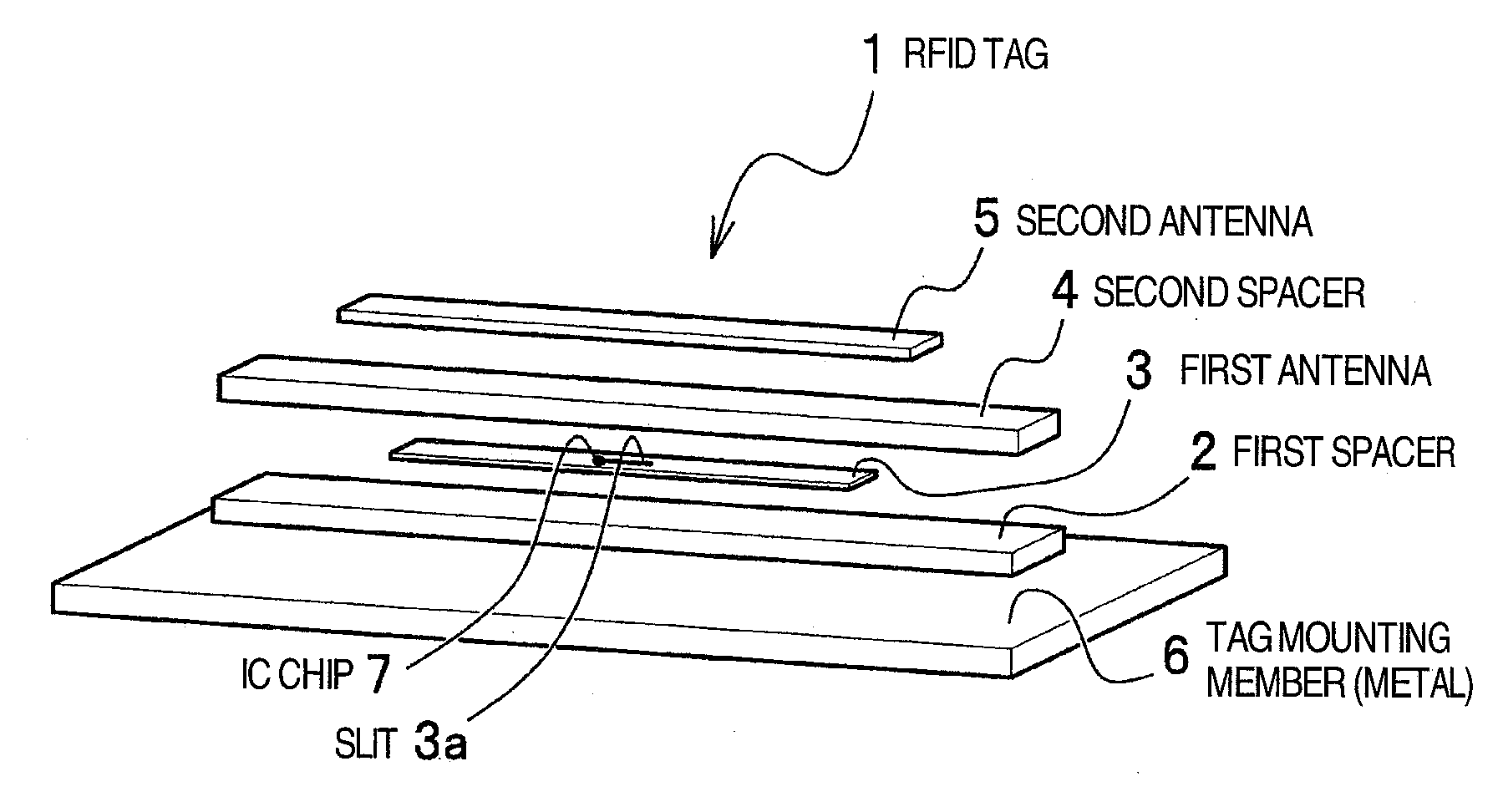
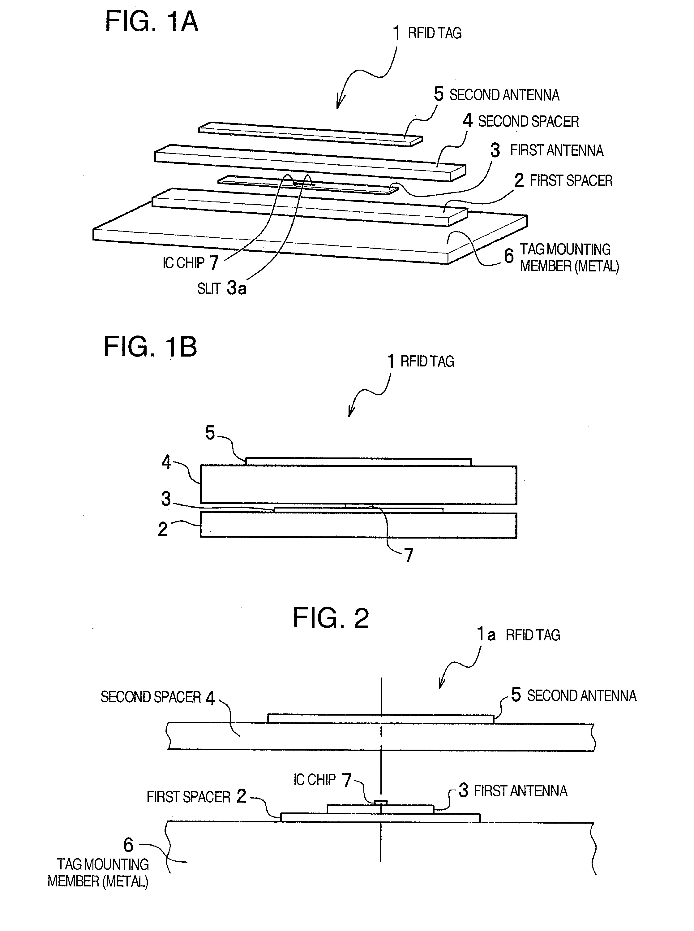
[0029]FIGS. 1A and 1B are block diagrams showing an RFID tag 1 according to a first embodiment of the present invention, in which FIG. 1A shows the state when the component elements are taken apart, and FIG. 1B shows the state when the component elements are stacked.

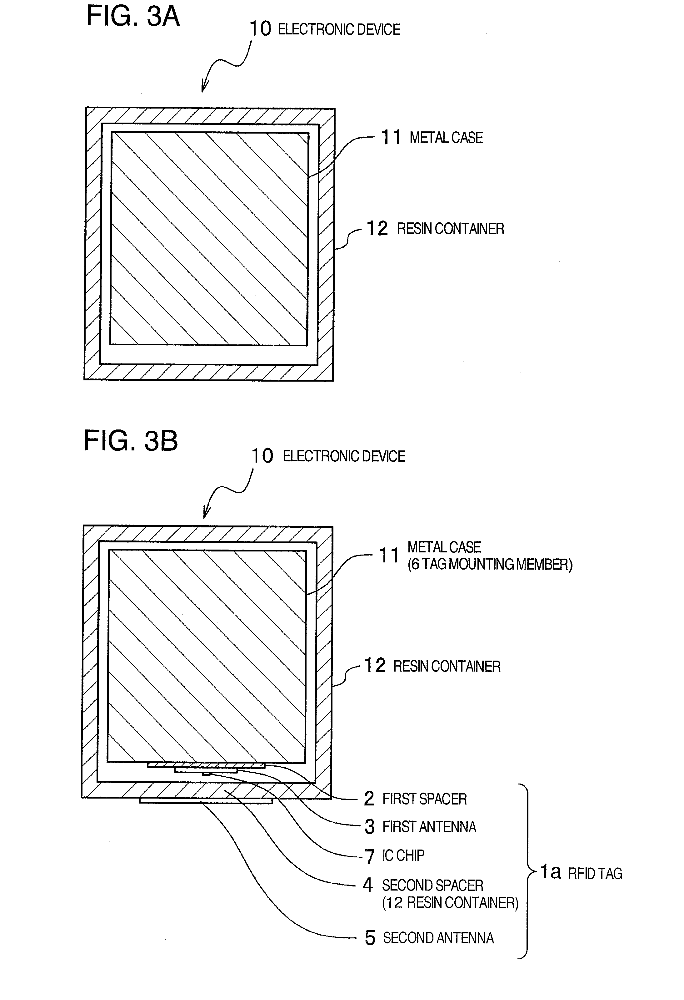
[0030]As will be described later with reference to FIGS. 3A and 3B, in an electronic device 10 structured to house a metal case 11 with an electronic circuitry accommodated therein in a resin container 12, a RFID tag 1a is formed in a thin structure suitable for its mounting by using a narrow clearance between the outer surface of the metal case 11 and the inner surface of the resin container 12. The resin container 12 is made of a synthetic resin in this case, but may be made of any other nonconductive material, such as a hard rubber or dried wood. The metal case 11 is formed of a metal such as aluminum or copper and used to perform electromagnetic shielding inside and outside of the metal case. The RFID tag 1a in this ...

second embodiment

[0066]FIG. 11 is a transparent plan view of an electronic device 10 including an RFID tag 1b according to a second embodiment of the present invention.

[0067]An RFID tag 1b according to the second embodiment can be mounted appropriately when the clearance between the metal case 11 and the resin container 12 in an electronic device 10 is a little wider. In other words, the first spacer 2 and the first antenna 3 are attached to the outer surface of the metal case 11 with an adhesive, and furthermore the second antenna 5 is attached to the inner surface of the resin container 12 at a position thereof facing the first antenna 3. In this case, the space between the first antenna 3 and the second antenna 5 serves as the second spacer 4. In other words, the air with a relative permittivity of 1 acts as the second spacer 4, but since the communication distance of the first antenna 3 is enough for waves to reach the second antenna 5, high-intensity electric waves can be radiated from the seco...

third embodiment

[0068]FIG. 12 is a transparent plan view of an electronic device 10 including an RFID tag 1c according to a third embodiment of the present invention.

[0069]In the RFID tag 1c according to the third embodiment, the first antenna 3 is attached directly to the inner surface of the resin container 12 without any intermediary, such as the first spacer 2 (refer to FIG. 3). And, the second antenna 5 is attached to the outer surface of the resin container 12 at a position thereof facing the first antenna 3.

[0070]According to the RFID tag 1c of the third embodiment, the RFID tag 1c can be mounted even when the clearance between the metal case 11 and the resin container 12 is narrow.

[0071]As has been described, an RFID tag according to the present invention includes a first antenna 3 on which an IC chip is mounted and a second antenna 5 that resonates at a prescribed frequency with the first antenna 3, and the first antenna 3 and the second antenna 5 are structured so as to be separated from ...


PUM


Abstract

A RFID tag for accommodation in a narrow clearance in an electronic device and providing a predetermined communication distance even if a displacement occurs between first and second antennas. First antenna is mounted through first spacer to metal case surface and second antenna mounted to resin container surface facing the first antenna. The dielectric resin container functions as a second spacer. Only the first spacer and first antenna are accommodated in the narrow clearance between metal case and resin container, the tag can be mounted even in an electronic device with a small redundant space and small size. First antenna is shorter than second antenna so that a required communication distance may be obtained even if their relative position is changed.

Description

CROSS-REFERENCE TO RELATED APPLICATIONS[0001]This application contains subject matter which is related to the subject matter of Ser. No. ______ filed on Apr. ______, 2007 in the name of Isao Sakama, claiming the priority from Japanese application JP-A-2006-149118 filed on May 30, 2006, entitled “IC TAG AND INLET FOR IC TAG” (note: Asamura's reference No. W3791-01EU), and assigned to the same assignee as this application. The content of Ser. No. ______ is hereby incorporated by reference in its entirety into this application.INCORPORATION BY REFERENCE[0002]The present application claims priority from Japanese application JP2006-216091 filed on Aug. 8, 2006, the content of which is hereby incorporated by reference into this application.BACKGROUND OF THE INVENTION[0003]The present invention relates to an RFID (Radio Frequency Identification) tag to transmit information, such as identification information (ID) recorded in an IC chip, on radio frequencies (RF), and particularly to an RFI...

Claims


Application Information

Patent Timeline
IPC IPC(8): G08B13/14
CPCG06K19/07749G06K19/07771G06K19/07767G06K19/00G06K19/07G06K19/077
Inventor SAKAMA, ISAO
Owner HITACHI LTD
Why Eureka
Try Eureka