Three-dimensional display device

a display device and three-dimensional technology, applied in the field of three-dimensional image display devices, can solve the problems of low resolution, moire, and the like, and achieve the effect of improving the stereoscopic effect and low resolution

Inactive Publication Date: 2008-02-14
HITACHI DISPLAYS
View PDF6 Cites 33 Cited by
  • Summary
  • Abstract
  • Description
  • Claims
  • Application Information

AI Technical Summary

Benefits of technology

[0006] Because of the principles of the IP method, three-dimensional image display devices based on the IP method are capable of displaying a stereoimage with a greatly improved stereoscopic effect in comparison with those based on the other methods. However, the IP method has the following problems: the resolution is low; a range within which a three-dimensional image can be identified (hereinafter referred to as a “visual field”) is not sufficient; color moire occurs; and the like.

Problems solved by technology

However, the IP method has the following problems: the resolution is low; a range within which a three-dimensional image can be identified (hereinafter referred to as a “visual field”) is not sufficient; color moire occurs; and the like.
Although the technique disclosed in the document (2) has improve the color moire problem, the improvement in visual field, the improvement in resolution, and the like, are not achieved.
Even if the color moire is improved, if a visual field is not sufficient, it is not possible to overcome the problem of a viewpoint that must be kept fixed.
Moreover, if the required resolution is not achieved, it is not possible to acquire a three-dimensional image with high image quality.

Method used


Image

  • Three-dimensional display device
  • Three-dimensional display device
  • Three-dimensional display device

Examples


first embodiment

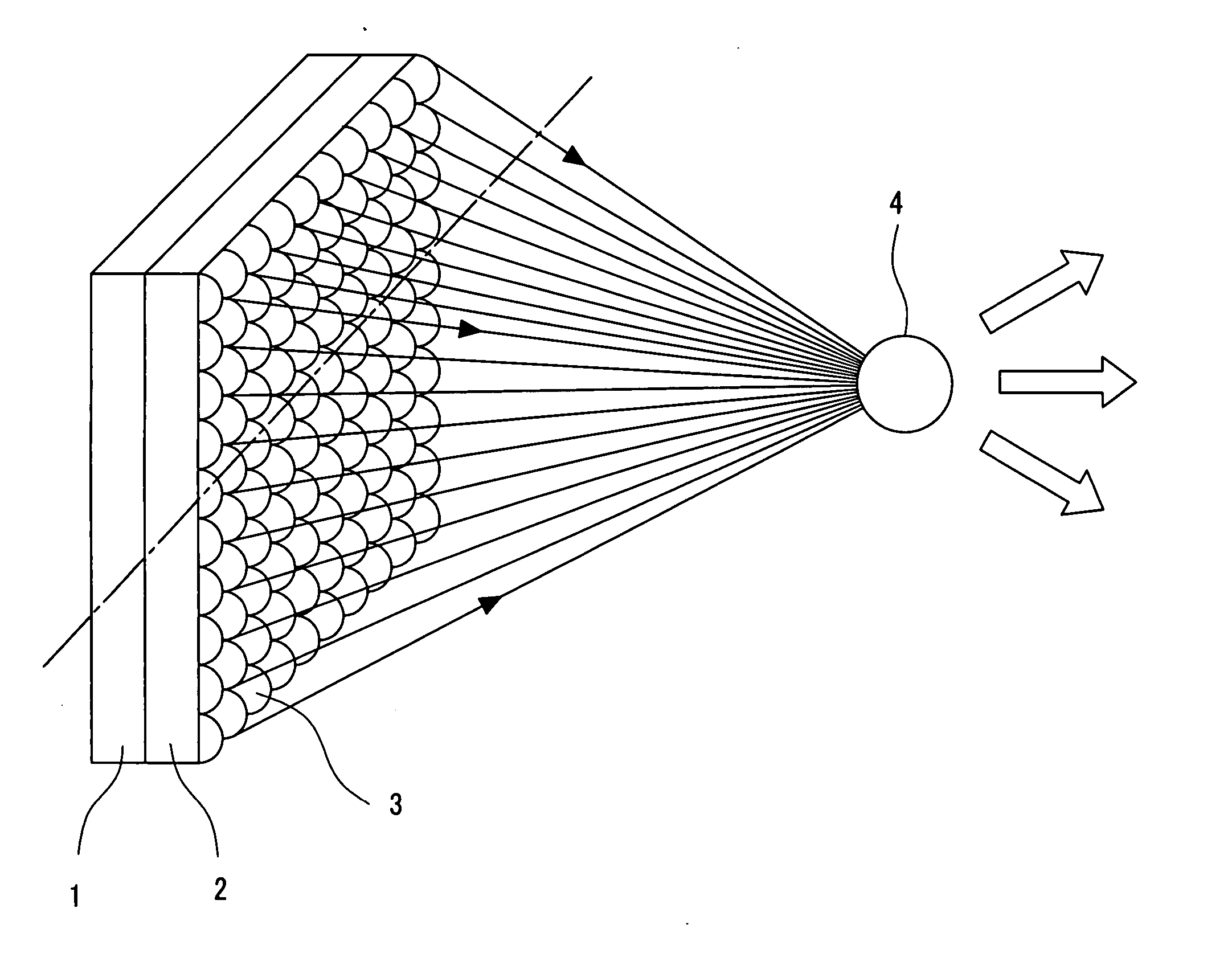
[0059]FIG. 1 is a diagram illustrating a basic configuration. A lens array 2 constituted of a large number of microlenses 3 is disposed on a two-dimensional image display device 1. The two-dimensional image display device 1 in this embodiment is a liquid crystal display panel. The two-dimensional image display device 1 generates a light spot 4 at an arbitrary position from the plurality of micro lenses 3. Under the lens array 2, there are a plurality of pixels, which form a light spot 4.

[0060] In conventional techniques, pixels, which emit or output red, green, and blue light, are disposed under each micro lens 3. However, according to the present invention, color filters colored with only one color are disposed under each micro lens 3. In this embodiment, the expression “under the micro lens 3” does not mean “directly under the micro lens 3”. For example, there is also a case where a light beam may be diagonally emitted in an area around a screen. In this case, a filter or a pixel...

second embodiment

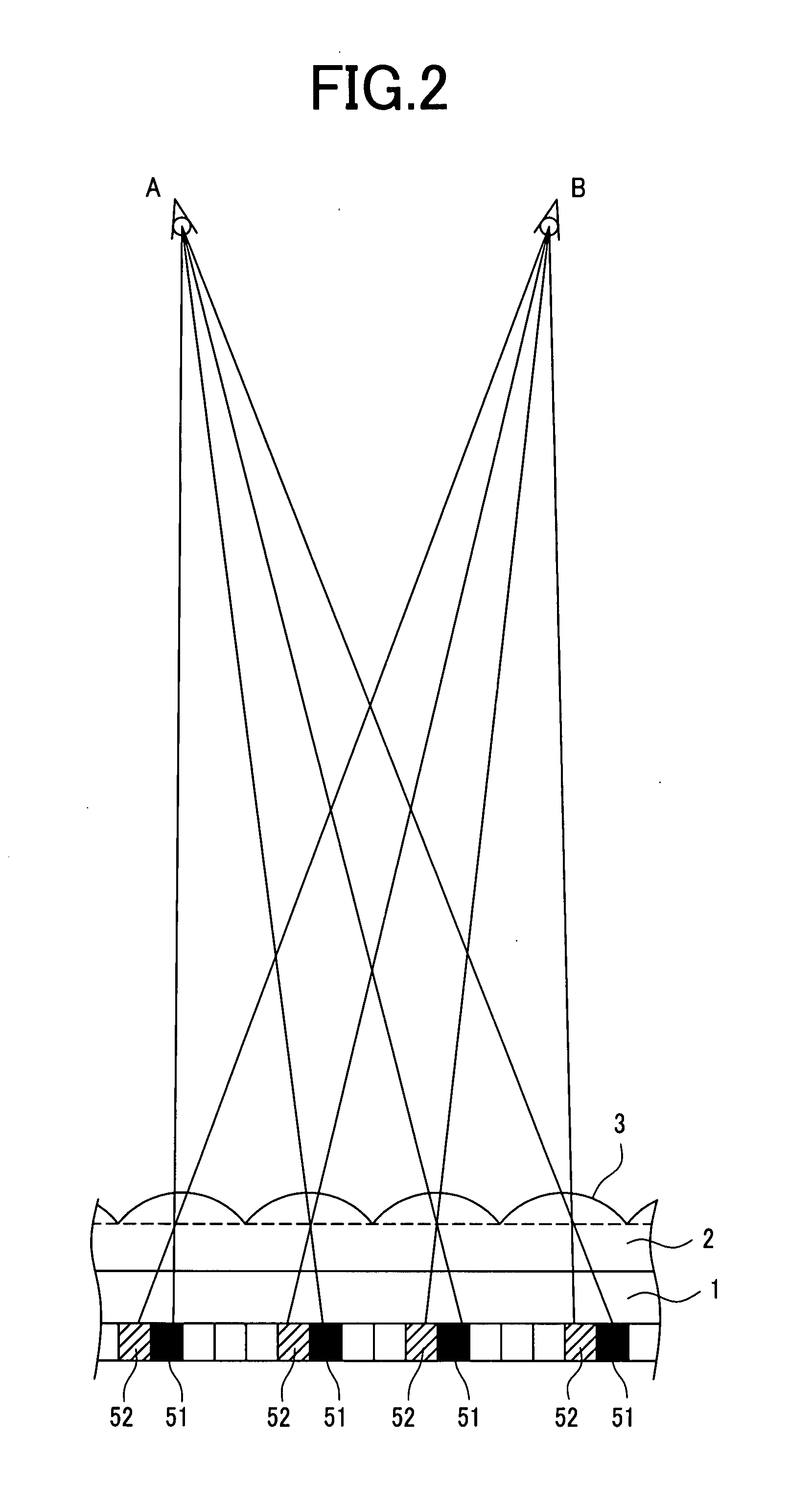
[0083]FIG. 8 is a diagram illustrating a second embodiment. An overall configuration of the second embodiment is the same as that of the first embodiment shown in FIG. 1. In addition, as is the case with the first embodiment, the liquid crystal display unit 50 is used. Elements in the liquid crystal display unit are also configured in the same manner as those of the first embodiment. In the second embodiment, with a direction of the lens array 2 being reverse to that of the first embodiment, the micro lenses 3 are disposed on the color filter substrate 52 side of the liquid crystal display unit 50. As a result, the distance between the color filter 60 and the micro lens 3 is decreased.

[0084] In FIG. 8, a light beam coming from the color filter 60 located around each of the micro lenses 3 travels in a straight line toward the center of the micro lens 3 in question. In the second embodiment, the distance from the color filter 60 to the center of the micro lens 3 is shortened because ...

third embodiment

[0088]FIG. 9 is a diagram illustrating a third embodiment. In the third embodiment, a bottom emission type organic EL display device 70 is used as the two-dimensional image display device 1. FIG. 10 is a cross sectional view illustrating one pixel of the bottom emission type organic EL display device 70.

[0089] In FIG. 10, an undercoat 72 is formed on a glass substrate; and a semiconductor layer 73 constituting a TFT is formed on the undercoat 72. A gate insulating film 74 is formed to cover the semiconductor layer 73; and a gate electrode 75 is formed on the gate insulating film 74. Interlayer insulation film 76 is formed to cover the gate electrode 75. Source drain (SD) wiring 77, which is the same layer as signal wiring, is formed on the interlayer insulation film 76. The SD wiring layer 77 is connected to a drain of the semiconductor layer 73 through a through hole that is formed in the interlayer insulation film 76 and the gate insulating film 74. A passivation film 78 used to ...


PUM


Abstract

Objects of the present invention are to widen a visual field of a three-dimensional image display device, and to improve the image quality of the three-dimensional image display device.
A number of pixels 51, 52 are formed on a two-dimensional image display device 1 for providing image data of a three-dimensional image. A lens array2 constituted of a large number of micro lenses 3 is disposed on the two-dimensional image display device 1. Each of the micro lenses 3 is associated with a plurality of pixels 5, each of which emits the same color. In order to ensure a visual field θ required for the three-dimensional image, a diameter LD of each of the micro lenses 3, the distance DFL between each of the pixels 5 and each of the micro lenses 3 in the two-dimensional image display device, are properly set.

Description

CLAIM OF PRIORITY [0001] The present application claims priority from Japanese Application JP 2006-199773 filed on Jul. 21, 2006, the content of which is hereby incorporated by reference into this application. BACKGROUND OF THE INVENTION [0002] The present invention relates to three-dimensional image display devices, and more particularly to autostereoscopic display. [0003] The autostereoscopic display are display devices that enable an observer to view a stereoimage without requiring the observer to use a particular tool such as glasses. As methods applied to the autostereoscopic display, there are various kinds of methods including the lenticular lens method and the holography method. However, the most of the methods are based on the principles that information on a light beam entering the eyes of an observer is controlled so that information on the light beam entering the left eye differs from information on the light beam entering the right eye, and the naked-eye stereoscopic vi...

Claims


Application Information

Patent Timeline
Patent Type & Authority Applications(United States)
IPC IPC(8): G06T15/00G02B30/10G03B35/00G03B35/18H04N13/04
CPCG02B3/0006G02F1/133526G02B27/22G02B30/10
Inventor KOIKE, TAKAFUMIOIKAWA, MICHIOUTSUGI, KEIYAMASAKI, MASAMI
Owner HITACHI DISPLAYS
Why Eureka
Try Eureka