Wideband modulated signal generating device

a modulated signal and wideband technology, applied in the direction of electrical equipment, optics, instruments, etc., can solve the problems of deteriorating the quality of demodulated signals, phase noise is also demodulated to become substantial white noise (intensity) noise, and the frequency of demodulated signals is increased. achieve the effect of optimally controlling bias voltage and desirable modulation characteristics

Inactive Publication Date: 2008-02-14
PANASONIC CORP
View PDF2 Cites 25 Cited by
  • Summary
  • Abstract
  • Description
  • Claims
  • Application Information

AI Technical Summary

Benefits of technology

[0029] Therefore, an object of the present invention is to provide specific means for optimally controlling bias voltages even if DC drift occurs where the frequency of the electric signal inputted to the optical SSB modulator is relatively low (on the order of 1 GHz), and to realize a wideband modulated signal generating device having desirable modulation characteristics.

Problems solved by technology

However, a light source such as a semiconductor laser typically has greater phase noise (a greater oscillation spectral line width) as compared with an electric oscillator.
When an angle-modulated signal is demodulated, the phase noise is also demodulated to become substantial white (intensity) noise.
Thus, the conventional wideband modulated signal generating device has the characteristic problem that the quality of the demodulated signal deteriorates significantly due to the noise.
Thus, the conventional device has the characteristic problem that it requires a complicated component such as a control circuit for monitoring / adjustment (e.g., the optical frequency control section 900).
For example, for an optical SSB modulator capable of performing a single-sideband suppressed-optical carrier modulation, there are very limited bias conditions under which carrier light or unnecessary sideband light components are canceled out by each other, whereby unnecessary light components are produced even by slight changes in the bias voltage.
Thus, even when the bias voltage does not change, the optimal point of operation may shift over time, thus producing unnecessary light components.
When an angle-modulated signal including such unnecessary wave components is demodulated, the distortion characteristics may be deteriorated (see, for example, Non-Patent Document 2).
However, the monitoring cannot always be done successfully.
However, where the frequency of the input signal is on the order of 1 GHz, there is no existing optical filter capable of separating light components arranged with small intervals therebetween.
Therefore, where the optical SSB modulator 3003 is driven with an input signal whose frequency is on the order of 1 GHz, it is impossible to control the bias voltages by monitoring the power of the carrier light and that of the unnecessary sideband light.
This cannot be done if the light components cannot be separated from each other.

Method used


Image

  • Wideband modulated signal generating device
  • Wideband modulated signal generating device
  • Wideband modulated signal generating device

Examples


first embodiment

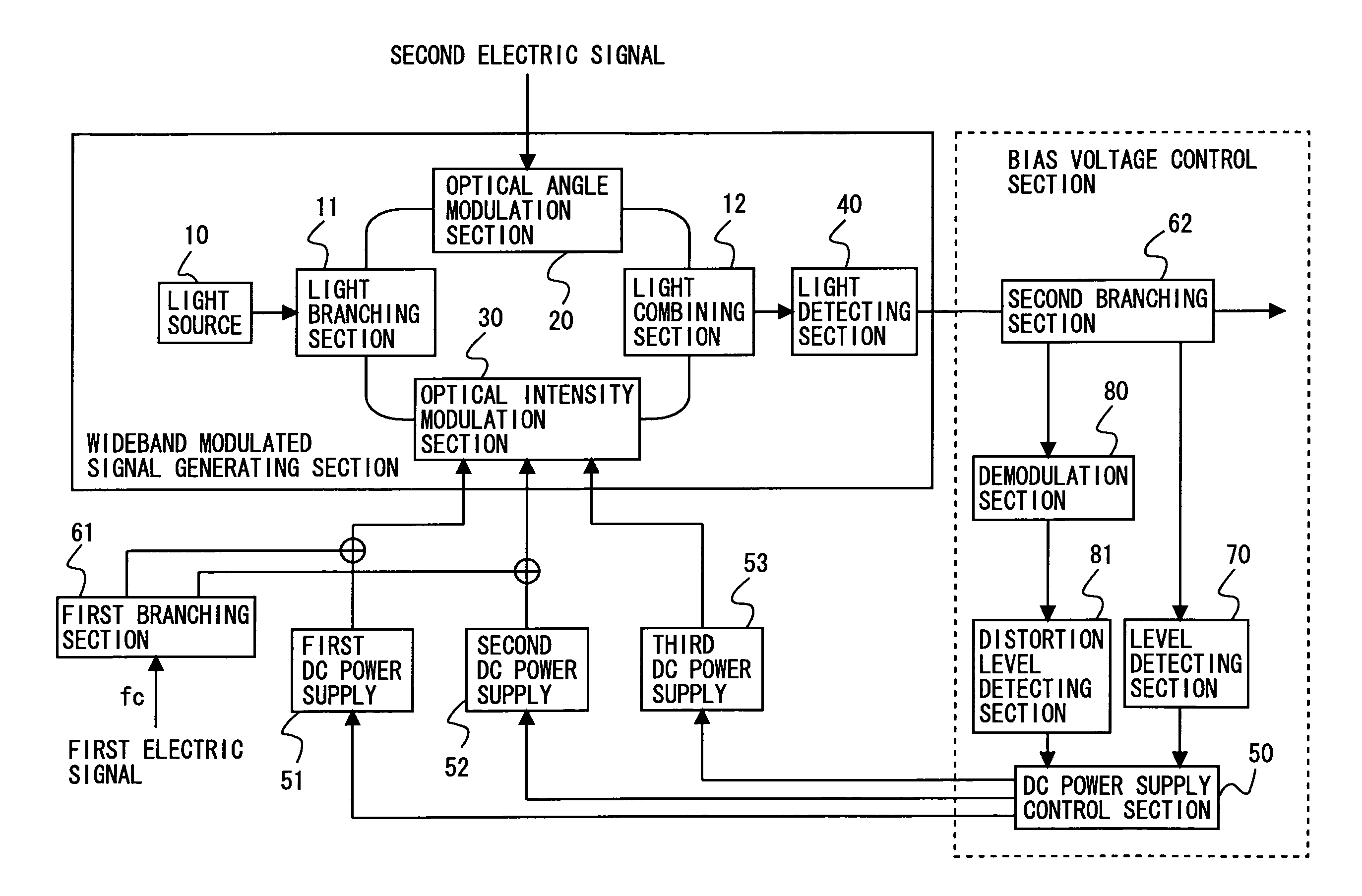
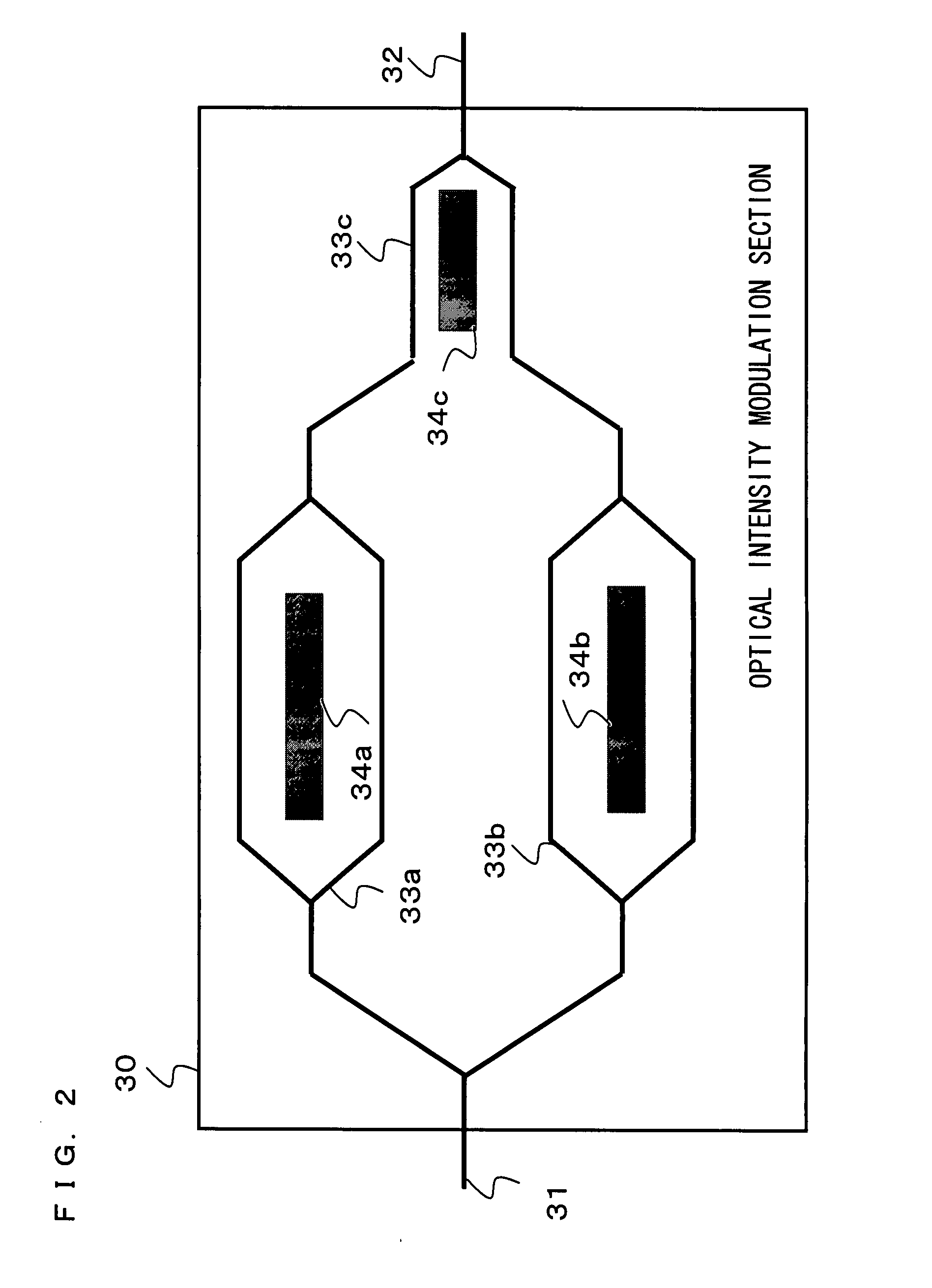
[0094]FIG. 1 is a block diagram showing a configuration of a wideband modulated signal generating device according to a first embodiment of the present invention. Referring to FIG. 1, the wideband modulated signal generating device includes a light source 10, a light branching section 11, a light combining section 12, an optical angle modulation section (an optical phase modulation section) 20, an optical intensity modulation section 30, a light detecting section 40, a DC power supply control section 50, a first DC power supply 51, a second DC power supply 52, a third DC power supply 53, a first branching section 61, a second branching section 62, a level detecting section 70, a demodulation section 80, and a distortion level detecting section 81. The light source 10, the light branching section 11, the light combining section 12, the optical angle modulation section 20, the optical intensity modulation section 30 and the light detecting section 40 may be referred to collectively as...

second embodiment

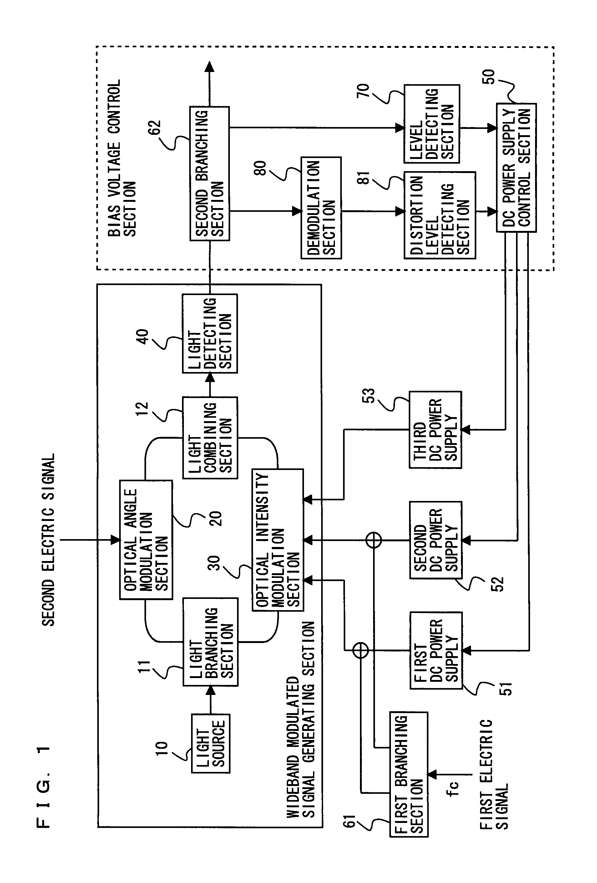
[0117]FIG. 8 is a block diagram showing a configuration of a wideband modulated signal generating device according to a second embodiment of the present invention. Referring to FIG. 8, the wideband modulated signal generating device includes the light source 10, the light branching section 11, the light combining section 12, the optical angle modulation section 20, the optical intensity modulation section 30, the light detecting section 40, the DC power supply control section 50, the first DC power supply 51, the second DC power supply 52, the third DC power supply 53, the first branching section 61, a third branching section 63, a fourth branching section 64, the level detecting section 70, the demodulation section 80, and the distortion level detecting section 81. The light source 10, the light branching section 11, the light combining section 12, the optical angle modulation section 20, the optical intensity modulation section 30 and the light detecting section 40 may be referred...


PUM

PropertyMeasurementUnit
frequencyaaaaaaaaaa
frequencyaaaaaaaaaa
frequencyaaaaaaaaaa

Abstract

The present invention provides a wideband modulated signal generating device capable of realizing an always stable operation and obtaining an intended wideband modulated signal in spite of a shift in the optimal bias voltage due to DC drift occurring in an optical intensity modulation section. In the wideband modulated signal generating device, a DC power supply control section 50 controls a first DC power supply 51 and a second DC power supply 52 for applying first and second bias voltages to an optical intensity modulation section 30 based on a signal level detected by a level detecting section 70, and controls a third DC power supply 53 for applying a third bias voltage to an optical intensity modulation section 30 based on a distortion level detected by a distortion level detecting section 81, thus compensating for a shift in the optimal bias voltage occurring due to DC drift.

Description

BACKGROUND OF THE INVENTION [0001] 1. Field of the Invention [0002] The present invention relates to a wideband modulated signal generating device for generating a wideband modulated signal (a phase-modulated signal or a frequency-modulated signal), and more particularly to a wideband modulated signal generating device using an external optical modulator capable of a bias voltage control of making the bias voltage applied to the external optical modulator follow the fluctuations of the optimal bias voltage due to DC drift. [0003] 2. Description of the Background Art [0004] Examples of conventional wideband modulated signal generating methods using the wideband property of light include a method for generating a wideband modulated signal through a heterodyne detection using the chirp characteristics of semiconductor lasers (e.g., Non-Patent Document 1). [0005] Non-Patent Document 1: K. Kikushima, et al., “Optical Super Wide-Band FM Modulation Scheme and Its Application to Multi-Chann...

Claims


Application Information

Patent Timeline
Patent Type & Authority Applications(United States)
IPC IPC(8): H04B10/04H04B10/12G02F1/01
CPCH04B2210/006H04B1/69
Inventor MASUDA, KOUICHIOHIRA, TOMOAKI
Owner PANASONIC CORP
Why Eureka
Try Eureka