
Circuit materials with improved bond, method of manufacture thereof, and articles formed therefrom

Active Publication Date: 2008-02-14
WORLD PROPERTIES
View PDF31 Cites 39 Cited by
  • Summary
  • Abstract
  • Description
  • Claims
  • Application Information

AI Technical Summary

Benefits of technology

[0008]In one embodiment, an adhesive useful for forming a circuit laminate comprises a poly(arylene ether), preferably a carboxy-functionalized poly(arylene ether), and a co-curable polybutadiene or polyisoprene polymer, preferably

Problems solved by technology

However, the polar groups in the epoxy resin also lead to a relatively high dielectric constant and high dissipation factor.
An unwanted consequence of the lower polarity of these resins systems is an inherently lower bond to metallic surfaces.
The presence of sulfur-containing compounds can be undesirable, giving rise to an increased tendency to corrode.
However, in practice it has been found that the elastomeric adhesion promoting layers can result in a soft surface, increasing the possibility of handling damage during processing.
As noted by Poutasse et al. in U.S. Pat. No. 5,629,098, adhesives that provide good adhesion to metal and substrate (as measured by peel strength) generally have less than satisfactory high temperature stability (as measured in a solder blister resistance test).
Conversely, adhesives that provide good high temperature stability generally have less than satisfactory adhesion.

Method used


Image

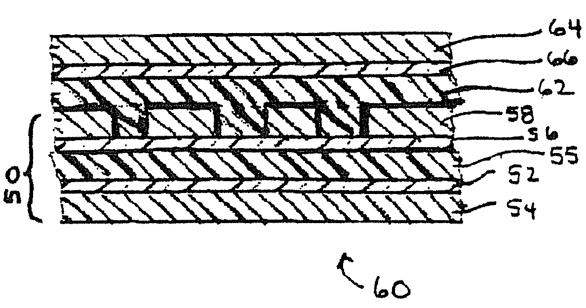
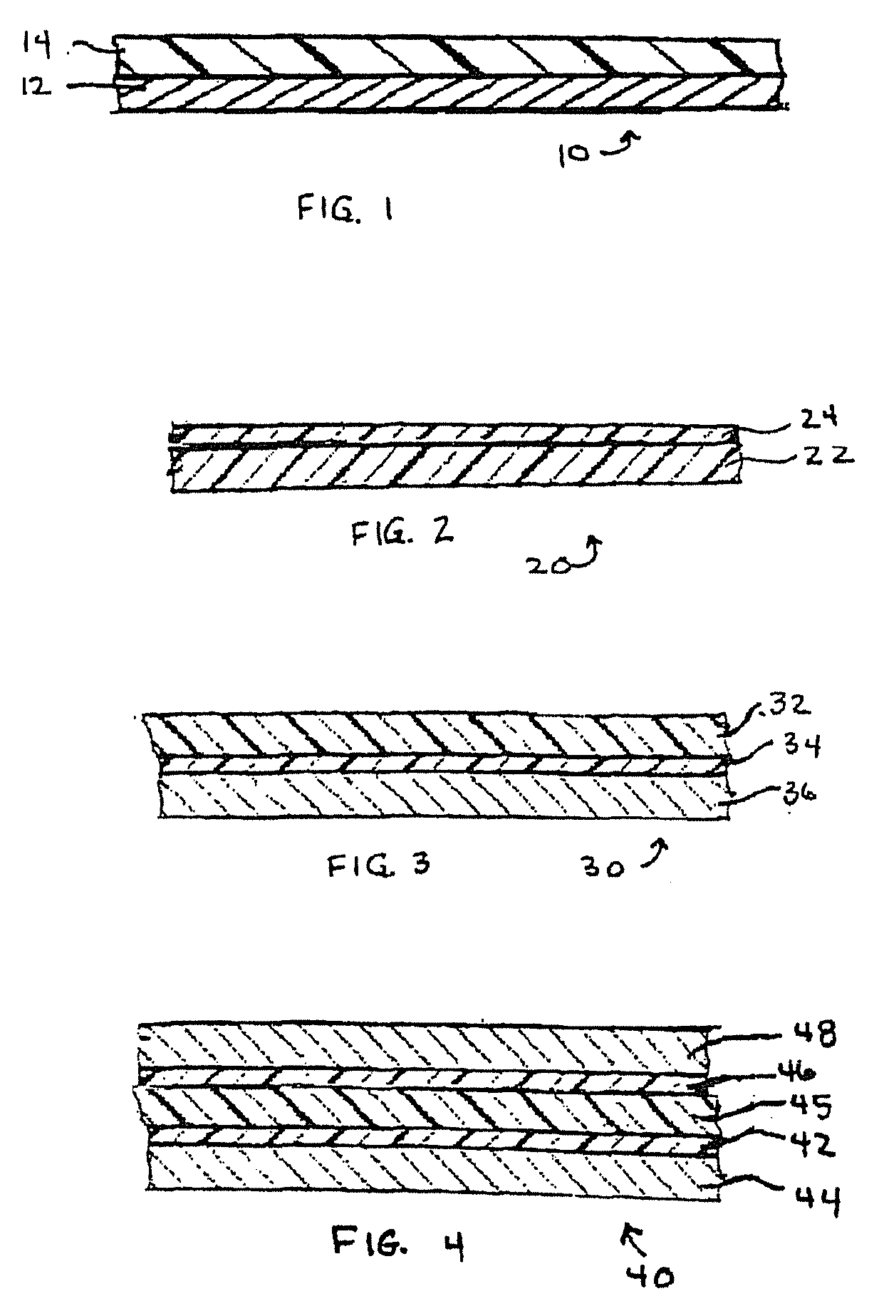
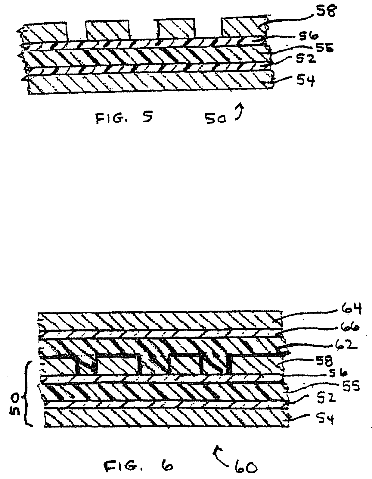
  • Circuit materials with improved bond, method of manufacture thereof, and articles formed therefrom
  • Circuit materials with improved bond, method of manufacture thereof, and articles formed therefrom
  • Circuit materials with improved bond, method of manufacture thereof, and articles formed therefrom

Examples


examples

[0080]The materials listed in Table 2 were used in the following examples.

TABLE 2Material nameChemical nameSupplierPPE-MAMaleinized polyphenylene etherAsahiBlendex HPP820Unmodified polyphenylene etherChemturaRicon ® 184MA6Butadiene-styrene copolymer adducted withSartomermaleic anhydrideHycar 2000 X168Vinyl-terminated polybutadieneNoveonTE 2000Polybutadiene with urethane linkagesNippon SodaB3000Vinyl-terminated polybutadieneNippon SodaBN1015Maleinated polybutadieneNippon SodaKraton ® D-1118SB diblock copolymer (20%) and SBS triblockShell Chemicalcopolymer (80%)RO-4350BFlame retardant thermosetting hydrocarbon-basedRogers Corp.circuit substrate materialRO-4233Thermosetting hydrocarbon-based circuitRogers Corp.substrate materialFRFlame retardant nonpolar circuit substratematerial containing Mg(OH)2 (U.S. Pat. No.7,022,404 to Sethumadhavan et al.)TOC-500Low profile standard copper, zinc freeOak-MitsuiTOC-500-LZLow profile copper, with light zinc flushOak-MitsuiTWSHigh profile copper foi...

examples 17-23

[0108]These Examples demonstrate the suitability of these adhesive formulations for effective and economical coating on standard production equipment, as well as the wide range of formulations over which the copper peel strength and high temperature resistance are improved.

[0109]Commercial scale coating trials of 25-inch (63.5-centimeter) wide rolls of copper foil were conducted on a slot die coater using the formulations shown in Table 8 (amounts shown are in grams). The six formulations we coated at line speeds of 30 feet / minute (fpm) (9.14 meter / minute) onto both Gould TWS high profile copper foil and Oak Mitsui MLS-TOC-500-LZ reverse-treated (low profile) copper foil (Ex. 17-Ex. 22). Formulation 20 was also coated at 60 fpm, simply to demonstrate that higher speed coating was possible (Ex. 23). The coating basis weights ranged from 6 to 8 gsm. The samples were dried in a three-zone in-line oven with drying temperatures of 100° C., 125° C., and 150° C. Approximately 250 linear fe...


PUM

PropertyMeasurementUnit
Lengthaaaaaaaaaa
Lengthaaaaaaaaaa
Frequencyaaaaaaaaaa

Abstract

A circuit material, comprising a conductive metal layer or a dielectric circuit substrate layer and an adhesive layer disposed on the conductive metal layer or the dielectric substrate layer, wherein the adhesive comprises a poly(arylene ether) and a polybutadiene or polyisoprene polymer.

Description

CROSS REFERENCE TO RELATED APPLICATION[0001]This application claims the benefits of U.S. Provisional Patent Application Ser. No. 60 / 821,710 filed Aug. 8, 2006, which is fully incorporated herein by reference.BACKGROUND[0002]This invention generally relates to circuit materials, methods of manufacture of the circuit materials, and articles formed therefrom.[0003]As used herein, a circuit material is an article used in the manufacture of circuits and multi-layer circuits, and includes circuit laminates, bond plies, resin coated conductive layers, and cover films. A circuit laminate is a type of circuit material that has a conductive layer, e.g., copper, fixedly attached to a dielectric substrate layer. Double clad circuit laminates have two conductive layers, one on each side of the dielectric substrate layer. Patterning a conductive layer of a laminate, for example by etching, provides a circuit. Multilayer circuits comprise a plurality of conductive layers, at least one of which con...

Claims


Application Information

Patent Timeline
IPC IPC(8): B32B7/12B05D5/12B32B27/04
CPCC08L71/126C08L15/00C09J107/00C08L71/12C08L19/006Y10T428/2804Y10T428/273H05K1/0393H05K2201/0158C09J171/12Y10T428/2883H05K2201/0133B32B7/12Y10T428/2878B32B15/14H05K2201/0355H05K3/386C08L2666/08C08L2666/14Y10T428/31696Y10T428/31511Y10T428/31855B05D7/16C09J171/02H05K3/38
Inventor PAUL, SANKAR K.
Owner WORLD PROPERTIES
Learn More