Programmable Logic Device and Method for Designing the Same

a logic device and logic technology, applied in the direction of instruments, computations using denominational number representation, pulse techniques, etc., can solve the problems of waste of space and inability to achieve low electric power consumption, and achieve the effect of reducing power consumption, small area, and reducing electric power consumption

Inactive Publication Date: 2008-02-21
SOCIONEXT INC
View PDF4 Cites 15 Cited by
  • Summary
  • Abstract
  • Description
  • Claims
  • Application Information

AI Technical Summary

Benefits of technology

[0023]According to the third invention, an application can be implemented in such a manner that a circuit portion requiring high speed is implemented by the first logical elements while a circuit portion operating at low speed is implemented by the second logical elements. Accordingly, the application can be implemented with a smaller area and lower power consumption compared with the case where all the circuit is implemented by the first logical elements.
[0024]According to the fourth invention, a clock signal with a low speed clock frequency is supplied to the logical elements designed for low speed operation, so that electric power consumption caused by a high speed clock frequency can be suppressed to achieve further lower electric power consumption.
[0025]According to the fifth invention, when the circuit portion requiring high speed in the application to be implemented is implemented by the first logical elements, wires can be arranged efficiently between the first logical elements requiring high speed communication to thereby achieve reduction in area of the programmable logic device at the time of mapping.
[0026]According to the sixth invention, a circuit requiring high speed operation is collectively disposed in the center portion for an applicati...

Problems solved by technology

As a result, the logical elements designed for high speed are also used for the circuit block operating at a low speed, so that it is impossible to achieve low electric power consumption...

Method used


Image

  • Programmable Logic Device and Method for Designing the Same
  • Programmable Logic Device and Method for Designing the Same
  • Programmable Logic Device and Method for Designing the Same

Examples


first embodiment

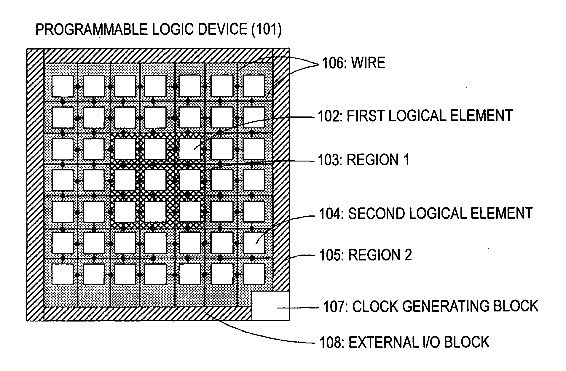
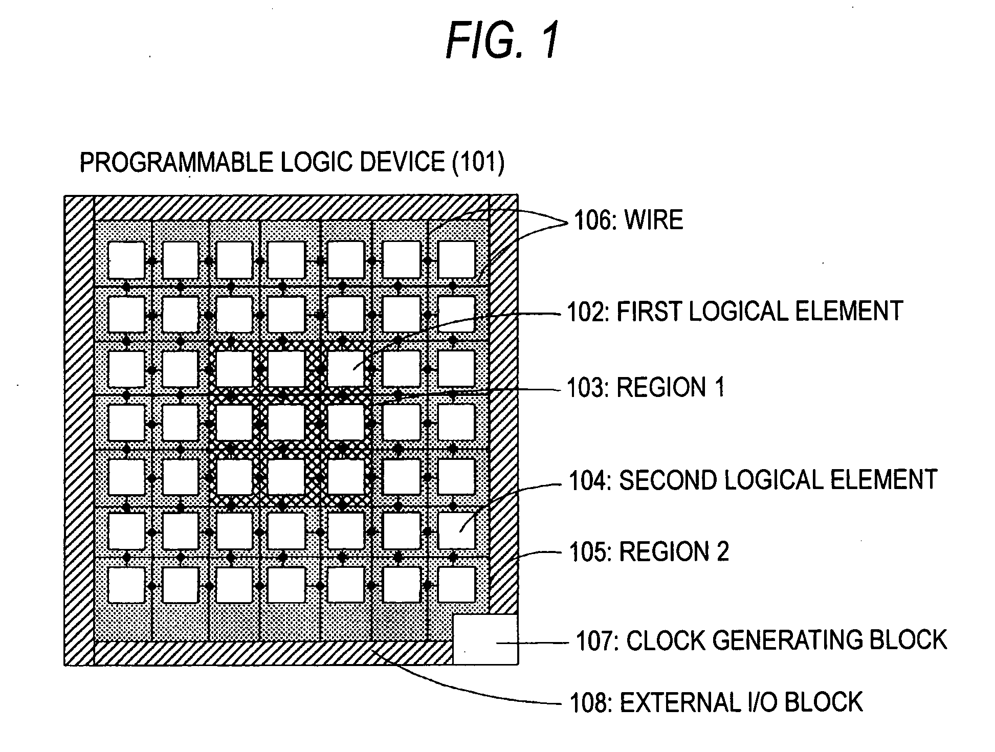
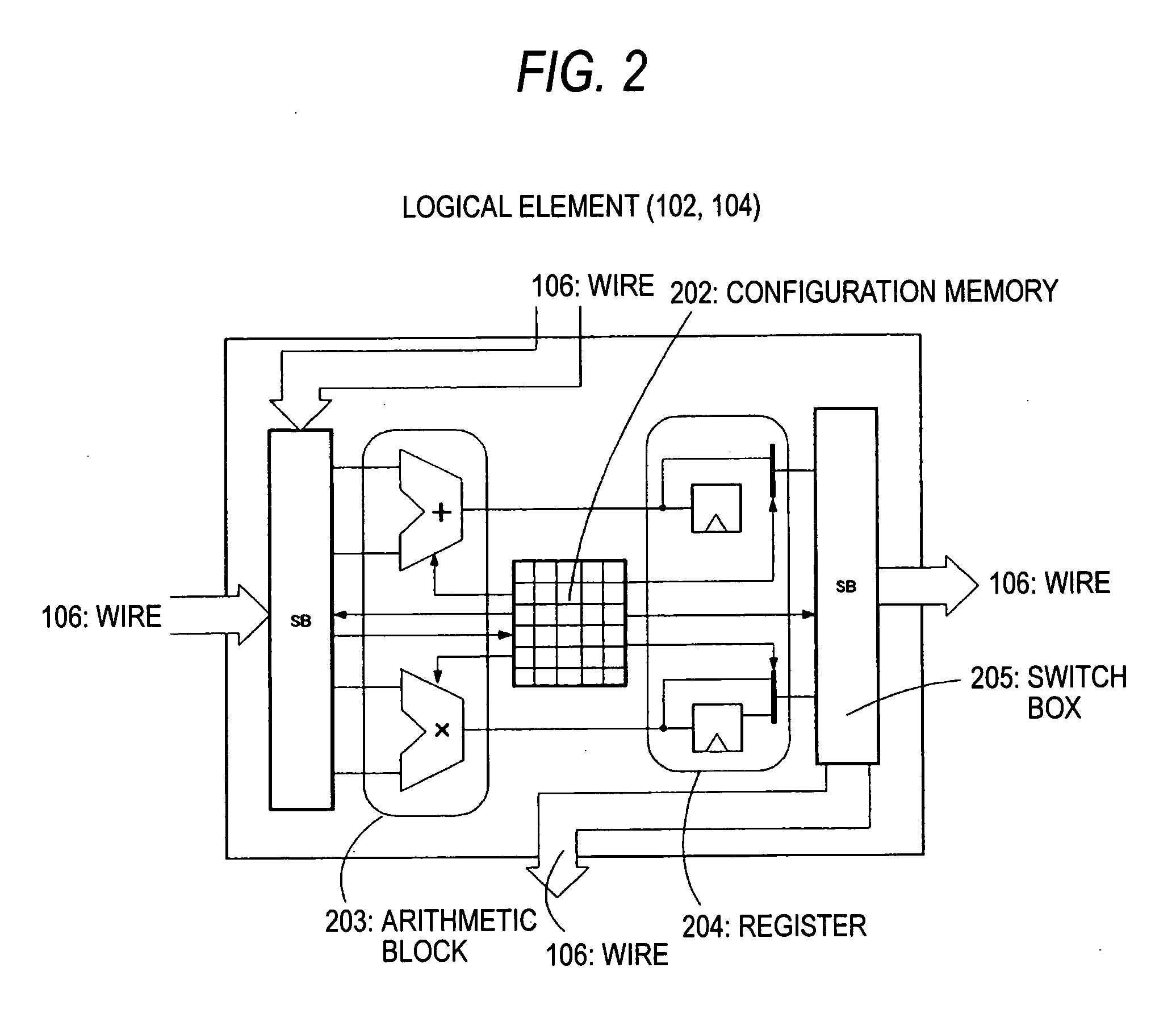
[0034]FIG. 1 is a configuration view showing a programmable logic device according to a first embodiment. In FIG. 1, a programmable logic device 101 includes a region 1 (103), a region 2 (105), wires 106, a clock generating block 107, and an external I / O block 108. The region 1 (103) includes a plurality of first logical elements 102 arranged. The region 2 (105) includes a plurality of second logical elements 104 arranged. Although each second logical element 104 has the same logical structure and function as each first logical element 102, each second logical element 104 is formed from transistors which constitute a circuit and which are higher in threshold voltage than those of each first logical element 102. The wires 106 are disposed horizontally and vertically between the first logical elements 102 or the second logical elements 104 so that the first logical elements 102 or the second logical elements 104 are connected to one another by the wires 106. The clock generating block...

second embodiment

[0042]FIG. 3 is a configuration view showing a programmable logic device according to a second embodiment. In FIG. 3, a programmable logic device 301 includes a region 1 (303), a region 2 (305), wires 306, a clock generating block 307, and an external I / O block 308. The region 1 (303) includes a plurality of first logical elements 302 arranged. The region 2 (305) includes a plurality of second logical elements 304 arranged. Although the logical structure and function of each second logical element 304 are quite the same as those of each first logical element 302, each second logical element 304 is formed from transistors which constitute a circuit and which are smaller in gate width W than each first logical element 302. The wires 306 are disposed horizontally and vertically between the first logical elements 302 or the second logical elements 304 so that the first logical elements 302 or the second logical elements 304 are connected to one another by the wires 306. The clock genera...

third embodiment

[0051]FIG. 4 is a configuration view showing a programmable logic device according to a third embodiment. In FIG. 4, a programmable logic device 401 includes a region 1 (402), a region 2 (403), and a clock generating block 404. The region 1 (402) includes a plurality of first logical elements arranged. The region 2 (403) includes a plurality of second logical elements arranged. Although the logical structure and function of each second logical element are quite the same as those of each first logical element, the upper limit of operating speed of the second logical element is designed to be lower than that of the first logical element. The clock generating block 404 outputs two different frequency clocks. Though not shown in the drawing, a high frequency clock is supplied to the logical elements in the first region 402 while a low frequency clock is supplied to the second logical elements in the second region 403.

[0052]In FIG. 4, configuration is made so that the region 2 (403) is d...


PUM


Abstract

The power consumption and area of a programmable logic device formed from programmable logical elements can be reduced.
In a programmable logic device 101 formed from programmable logical elements, there are provided first logical elements 102 and second logical elements 104 having the same logic as the first logical elements 102 but having an upper limit of operating speed designed to be lower than that of the first logical elements 102.

Description

TECHNICAL FIELD[0001]The present invention relates to a programmable logic device including a plurality of programmable logical elements arranged in rows and columns, and a method for designing the same.BACKGROUND ART[0002]The life cycles of products tend to become shorter and shorter because needs for information processing in information processing terminals have been diversified so that standards for communication systems and signal processing have changed kaleidoscopically in recent years. Devices having functions capable of being changed by programs are useful to cope with the shortening of the life cycles of products. A DSP (Digital Signal Processor) and a microprocessor are examples of these devices. In the DSP or microprocessor, an instruction program can be changed to provide the degree of freedom of the program in the instruction level. The DSP or microprocessor is however inferior in processing performance to an ASIC (Application Specified IC) limited to a specific purpos...

Claims


Application Information

Patent Timeline
IPC IPC(8): H03K19/177H01L21/8234H01L21/82H01L27/088H01L27/118
CPCH01L27/118
Inventor MORI, ATSUHIROMARUI, SHINICHIOKAMOTO, MINORU
Owner SOCIONEXT INC
Why Eureka
Try Eureka