Electro-optical device and electronic apparatus

a technology of electronic equipment and optical elements, applied in static indicating devices, instruments, electroluminescent light sources, etc., can solve the problems of reducing yield, affecting the desired operation of each unit circuit, and reducing the width of the window frame, so as to achieve the effect of suppressing the size of the driving circui

Inactive Publication Date: 2008-02-21
SEIKO EPSON CORP
View PDF7 Cites 34 Cited by
  • Summary
  • Abstract
  • Description
  • Claims
  • Application Information

AI Technical Summary

Benefits of technology

[0009]An advantage of some aspects of the invention is that it suppresses the size of a driving circuit.

Problems solved by technology

Thus, there is a problem that it needs to ensure a large space for arranging the driving circuit around the array of the electro-optical elements (that is, it is difficult to reduce the width of the window frame).
There is also a problem that a yield is reduced due to an increase in number of elements that form the driving circuit.
Incidentally, if the electro-optical element of the unit circuit initiates to operate during an initialization period when the initializing switching element of the unit circuit is in a conductive state, it may impede a desired operation of each unit circuit.
For example, if the electro-optical element initiates to operate before the potential of the gate of the driving transistor converges on an electric potential corresponding to its own threshold voltage, variation in threshold voltages of the driving transistors is not effectively compensated.
Furthermore, if the electro-optical element initiates to operate before the supply of reset potential to the gate of the driving transistor is completed, the electro-optical element cannot be driven to a desired gray-scale level.
Incidentally, if the electro-optical element of each unit circuit initiates to operate within a selection period during which a data signal is supplied to the unit circuit, it is difficult to control the electro-optical element to a desired gray-scale level with high accuracy.
In addition, there is also a problem that the amount of time required for appropriately writing ea data signal to the unit circuit is increased.

Method used


Image

  • Electro-optical device and electronic apparatus
  • Electro-optical device and electronic apparatus
  • Electro-optical device and electronic apparatus

Examples


first embodiment

A: First Embodiment

A-1: Configuration of Electro-optical Device

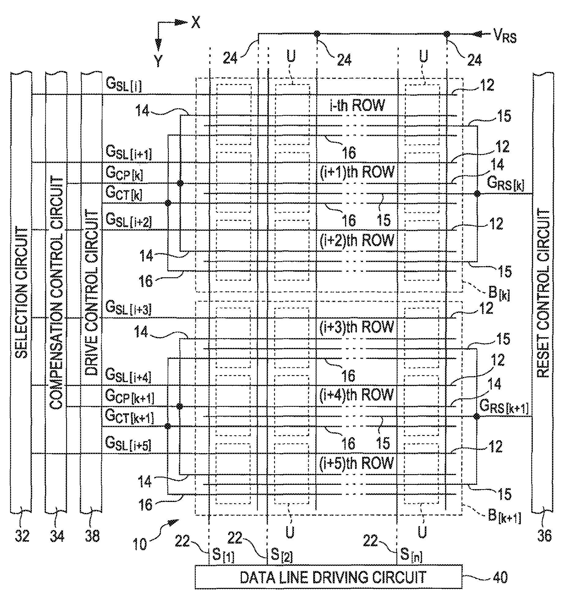
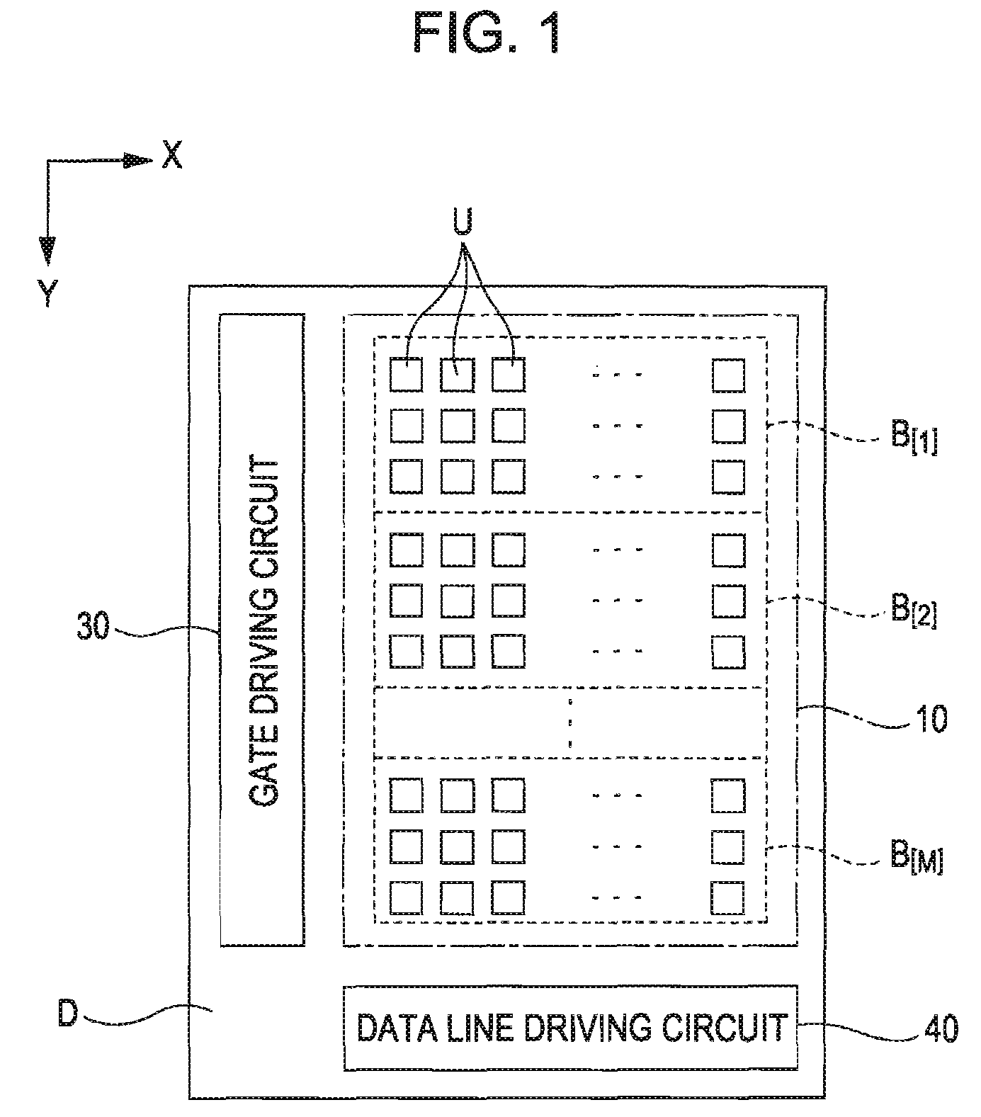
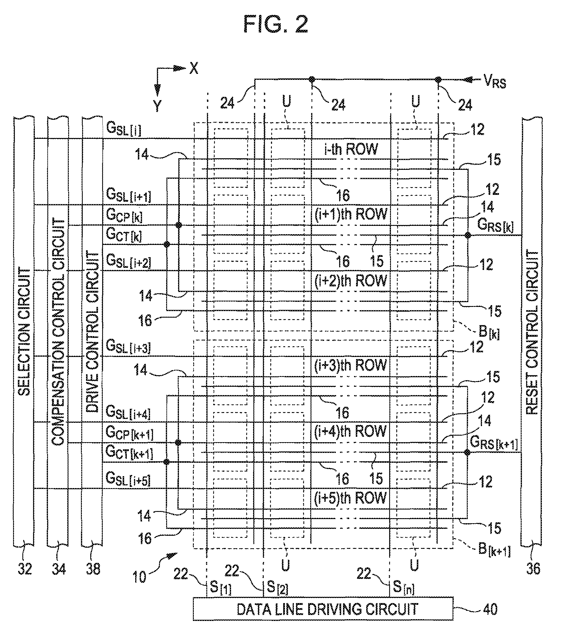
[0078]FIG. 1 is a block diagram of a configuration of an electro-optical device according to a first embodiment. The electro-optical device D is an image display device. The electro-optical device D includes an element array area 10, a gate driving circuit 30, and a data line driving circuit 40. A plurality of unit circuits (pixel circuits) U are arranged in the element array area 10. The gate driving circuit 30 drives the unit circuits U.

[0079]In the element array area 10, groups of n unit circuits U that are arranged in an X direction are arranged parallel to each other in a Y direction perpendicular to the X direction over m rows (n and m are natural numbers). That is, the plurality of unit circuits U are arranged in a matrix of horizontal m rows by vertical n columns. The unit circuits U are separated into M (M=m / 3) groups B[1] to B[M], each including three successive rows of unit circuits U in the Y direction. That ...

second embodiment

B: Second Embodiment

[0114]The following will describe a second embodiment of the invention. Note that the same reference numerals are assigned to the components of the present embodiment having the same or similar operation and function as those of the first embodiment, and a detailed description thereof is omitted where appropriate.

[0115]FIG. 7 is a block diagram showing a relation between each unit circuit IT and the gate driving circuit 30 according to the present embodiment. FIG. 8 is a timing chart showing waveforms of signals that are supplied to the unit circuits U. FIG. 7 shows only one group B[k] as an example.

[0116]As shown in FIG. 7 and FIG. 8, the drive control circuit 38 in the present embodiment generates drive control signals GCT[1] to GCT[m] for the corresponding m rows that form the element array area 10. The drive control signal GCT[i] is a signal that is in a low level during the non-selection period TOFF[i] when the start point is separately set on a row to row b...

third embodiment

C: Third Embodiment

[0120]The following will describe a third embodiment of the invention. Note that the same reference numerals are assigned to the components of the present embodiment having the same or similar operation and function as those of the first embodiment or second embodiment, and a detailed description thereof is omitted where appropriate.

[0121]FIG. 9 is a block diagram showing a relation between each unit circuit U and the gate driving circuit 30 according to the present embodiment. As shown in FIG. 9, the electro-optical device D of the present embodiment includes m regulator circuits 60 corresponding to the respective rows in addition to the components of the second embodiment. The i-th regulator circuit 60 is a device that delays the control signal G[k,i] output from the i-th NAND circuit 50, that is, the logic signal, relative to the compensation control signal GCP[k]. The regulator circuit 60 of the present embodiment includes two buffers 62 that are arranged in a...


PUM


Abstract

An electro-optical device may include a plurality of data lines, a plurality of selection lines, a plurality of unit circuits, a selection circuit, and a control circuit. Each of the plurality of unit circuits is connected to a corresponding one of the plurality of data lines and a corresponding one of the plurality of selection lines. The plurality of unit circuits form a unit circuit group for each of the selection lines. The selection circuit supplies a selection signal to one of the plurality of selection lines so that data signals are written from the plurality of data lines to the corresponding unit circuit group during a selection period when the corresponding unit circuit group is selected. The control circuit supplies a common control signal to the unit circuits included in a group consisting of two or more of the unit circuit groups. The control circuit brings the control signal into a predetermined state during a period that is different from the selection period when any one of the two or more unit circuit groups is selected. Here, each of the plurality of unit circuits includes an electro-optical element, a first switching element, a driving transistor. The first switching element writes the data signal from one of the plurality of data lines to the corresponding unit circuit in accordance with the selection signal. The gate of the driving transistor is supplied with a voltage corresponding to the data signal. The driving transistor supplies a driving current to the electro-optical element.

Description

[0001]The entire disclosure of Japanese Patent Application Nos: 2006-222292, filed Aug. 17, 2006, 2006-230184, filed Aug. 28, 2006, and 2007-164683, filed Jun. 22, 2007 are expressly incorporated by reference herein.BACKGROUND[0002]1. Technical Field[0003]The present invention relates to a technology for controlling an electro-optical element, such as a light emitting element, and an electronic apparatus.[0004]2. Related Art[0005]It has been proposed in the existing art that an electro-optical device that uses transistors (hereinafter, referred to as “driving transistors”) for driving electro-optical elements. For example, in the electro-optical device that employs a light emitting element, such as an organic light emitting diode, as an electro-optical element, the electric potential of the gate of each driving transistor is set (data writing) in correspondence with a data signal that specifies a gray-scale level of the electro-optical element. Then, the electro-optical elements are...

Claims


Application Information

Patent Timeline
Patent Type & Authority Applications(United States)
IPC IPC(8): G06F3/038H05B44/00
CPCG09G3/3233G09G3/325G09G3/3283G09G3/3291G09G2310/0218G09G2300/0819G09G2300/0852G09G2300/0861G09G2310/0216G09G2300/0426G09G3/30G09G3/20
Inventor KANDA, EIJI
Owner SEIKO EPSON CORP
Why Eureka
Try Eureka