Carbon precursors for use during silicon epitaxial film formation

a technology of carbon precursors and epitaxy materials, applied in the direction of crystal growth process, polycrystalline material growth, chemically reactive gases, etc., can solve the problems of epitaxy material deposition, difficult production of ultra shallow source/drain junctions, and limited, or no, deposition of polycrystalline materials

Inactive Publication Date: 2008-02-21
APPLIED MATERIALS INC
View PDF39 Cites 181 Cited by
  • Summary
  • Abstract
  • Description
  • Claims
  • Application Information

AI Technical Summary

Benefits of technology

[0011] In yet other aspects, the present invention provides a method of forming an epitaxial film on a substrate including providing a substrate, wherein the substrate is at least one of a silicon-on-insulator substrate and a bulk substrate, for use in recess source/drain metal oxide semiconductor field effect transistors; exposing the substrate to a silicon source and at least one of SiH2(CH3)2, SiH(CH3)3, Si(CH3)4, 1,3-disilabutane, and C2H2, so as to form an epitaxial film on at least a portion of the substrate; and exposing the substrate to an etchant so as to etch the epitaxial film and an

Problems solved by technology

As smaller transistors are manufactured, ultra shallow source/drain junctions are becoming more challenging to produce.
Therefore, by changing the concentration of an etchant gas, the net selective process results in deposition of epitaxy material and limited, or no, deposition of polycrystalline material.
On the other hand, the ultra shallow source/drain junction inevitably results in increased series resi

Method used


Image

  • Carbon precursors for use during silicon epitaxial film formation
  • Carbon precursors for use during silicon epitaxial film formation
  • Carbon precursors for use during silicon epitaxial film formation

Examples


example 1

Selective Epitaxy of Silicon with Cl2 Etchant

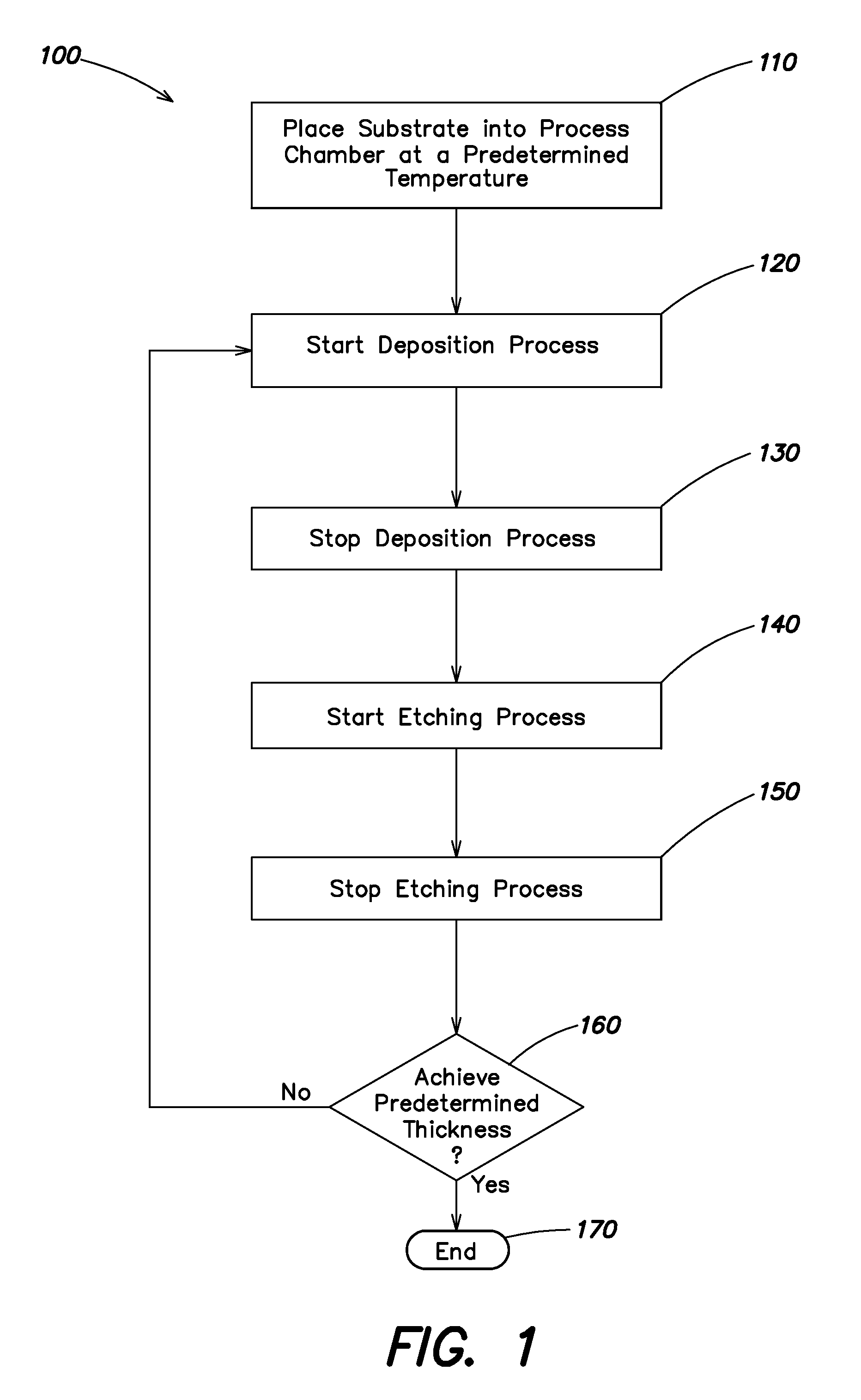
[0098] The substrate was placed into a process chamber heated and maintained at 550° C. The process chamber was maintained at a pressure of about 15 Torr. The substrate surface was exposed to a flow of deposition gas containing silane with a flow rate of 100 sccm and nitrogen with a flow rate of 25 slm for 7 seconds. The substrate was thereafter exposed to an etching gas containing chlorine gas with a flow rate of 20 sccm and nitrogen with a flow rate of 25 slm for 10 seconds. A cycle of deposition gas exposure and etching gas exposure was repeated 50 times to form an epitaxially grown silicon layer on the exposed monocrystalline portion of the substrate. The silicon epitaxial layer had a thickness of about 1,000 Å.

example 2

Selective Epitaxy of Silicon Germanium with Cl2 Etchant

[0099] The substrate was placed into a process chamber heated and maintained at 550° C. The process chamber was maintained at a pressure of about 15 Torr. The substrate surface was exposed to a flow of deposition gas containing silane with a flow rate of 100 sccm, germane with a flow rate of 3 sccm and nitrogen with a flow rate of 25 slm for 8 seconds. The substrate was thereafter exposed to an etching gas containing chlorine gas with a flow rate of 20 sccm and nitrogen with a flow rate of 25 μm for 10 seconds. A cycle of deposition gas exposure and etching gas exposure was repeated 50 times to form an epitaxially grown silicon-containing layer on the exposed monocrystalline portion of the substrate. The silicon-containing epitaxial layer had a thickness of about 1,700 Å.

example 3

Selective Epitaxy of Silicon Germanium with Cl2 Etchant

[0100] The substrate was placed into a process chamber heated and maintained at 550° C. The process chamber was maintained at a pressure of about 15 Torr. The substrate surface was exposed to a flow of deposition gas containing silane with a flow rate of 100 sccm and nitrogen with a flow rate of 25 slm for 7 seconds. The substrate surface was thereafter exposed to a flow of second deposition gas containing germane with a flow rate of 5 sccm and nitrogen with a flow rate of 25 slm for 7 seconds. The substrate was exposed to an etching gas containing chlorine gas with a flow rate of 20 sccm and nitrogen with a flow rate of 25 slm for 10 seconds. A cycle of deposition gas exposure and etching gas exposure was repeated 50 times to form an epitaxially grown silicon-containing layer on the exposed monocrystalline portion of the substrate. The silicon-containing epitaxial layer had a thickness of about 1,800 Å.


PUM


Abstract

The present invention provides systems and methods of forming an epitaxial film on a substrate. After heating in a process chamber, the substrate is exposed to a silicon source and at least one of SiH2(CH3)2, SiH(CH3)3, Si(CH3)4, 1,3-disilabutane, and C2H2, at a temperature of greater than about 250 degrees Celsius and a pressure greater than about 1 Torr so as to form an epitaxial film on at least a portion of the substrate. Then, the substrate is exposed to an etchant so as to etch the epitaxial film and any other films formed during the deposition. The deposition and etching may be repeated until a film of a desired thickness is achieved. Numerous other aspects are disclosed.

Description

[0001] The present application claims priority to U.S. Provisional Patent Application Ser. No. 60 / 785,740, filed Mar. 24, 2006 and entitled “CARBON PRECURSORS FOR USE DURING SILICON EPITAXIAL FILM FORMATION”, (Docket No. 10303 / L) which is incorporated by reference herein in its entirety for all purposes. CROSS-REFERENCE TO RELATED APPLICATIONS [0002] The present application is also related to U.S. patent application Ser. No. 11 / 001,774, filed Dec. 1, 2004 (Docket No. 9618) and U.S. patent application Ser. No. 11 / 227,974, filed Sep. 14, 2005 (Docket No. 9618 / P01), which are both hereby incorporated by reference herein in their entirety for all purposes.FIELD OF THE INVENTION [0003] Embodiments of the invention generally relate to the field of electronic manufacturing processes and devices, more particular, to methods of depositing silicon-containing films while forming electronic devices. BACKGROUND [0004] As smaller transistors are manufactured, ultra shallow source / drain junctions ...

Claims


Application Information

Patent Timeline
IPC IPC(8): H01L21/20
CPCC30B25/02C30B29/06H01L21/02529H01L21/02532H01L21/0262H01L29/7834H01L21/32134H01L29/66272H01L29/6656H01L29/66636H01L29/732H01L21/02636
Inventor SAMOILOV, ARKADII V.KODALI, ROHINIZOJAJI, ALIKIM, YIHWAN
Owner APPLIED MATERIALS INC
Why Eureka
Try Eureka