High Efficiency Solar Cells and Manufacturing Methods

a solar cell, high-efficiency technology, applied in the field of solar cells, can solve the problems of low conversion efficiency, high manufacturing cost, and low cost/watt of commercial photovoltaics, and achieve the effects of increasing the thickness of the absorber layer, and reducing the cost of manufacturing

Inactive Publication Date: 2008-02-28
BEAMREACH SOLAR INC
View PDF1 Cites 124 Cited by
  • Summary
  • Abstract
  • Description
  • Claims
  • Application Information

AI Technical Summary

Problems solved by technology

One of the key limitations to the wide-spread implementation of solar cells is their relatively low conversion efficiency (and another limitation is a relatively high manufacturing cost).
As a result, the cost / watt of commercial photovoltaics is not competitive with fossil fuels and various conventional forms of grid-distributed electricity.
Large scale implementation of commercial photovoltaics as a sustainable energy source has been plagued by its economics that are not yet fully cost-competitive with conventional energy sources.
However, the cost of single crystal silicon has remained high while supplies have tightened due to increasing demand from the IC industry.
While these 2nd generation thin-film PV cells are promising, their efficiencies are still in the range of 10%-13%, thus still not making them a compelling replacement for the expensive but dominant single-crystal silicon cells.

Method used


Image

  • High Efficiency Solar Cells and Manufacturing Methods
  • High Efficiency Solar Cells and Manufacturing Methods
  • High Efficiency Solar Cells and Manufacturing Methods

Examples


Embodiment Construction

[0029]The following description is not to be taken in a limiting sense, but is made for the purpose of describing the general principles of the disclosure. The scope of the disclosure should be determined with reference to the claims.

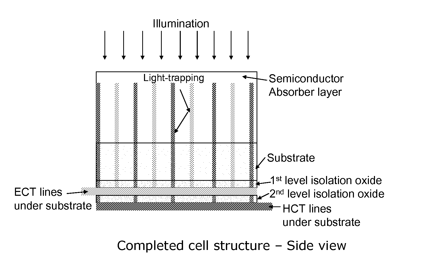
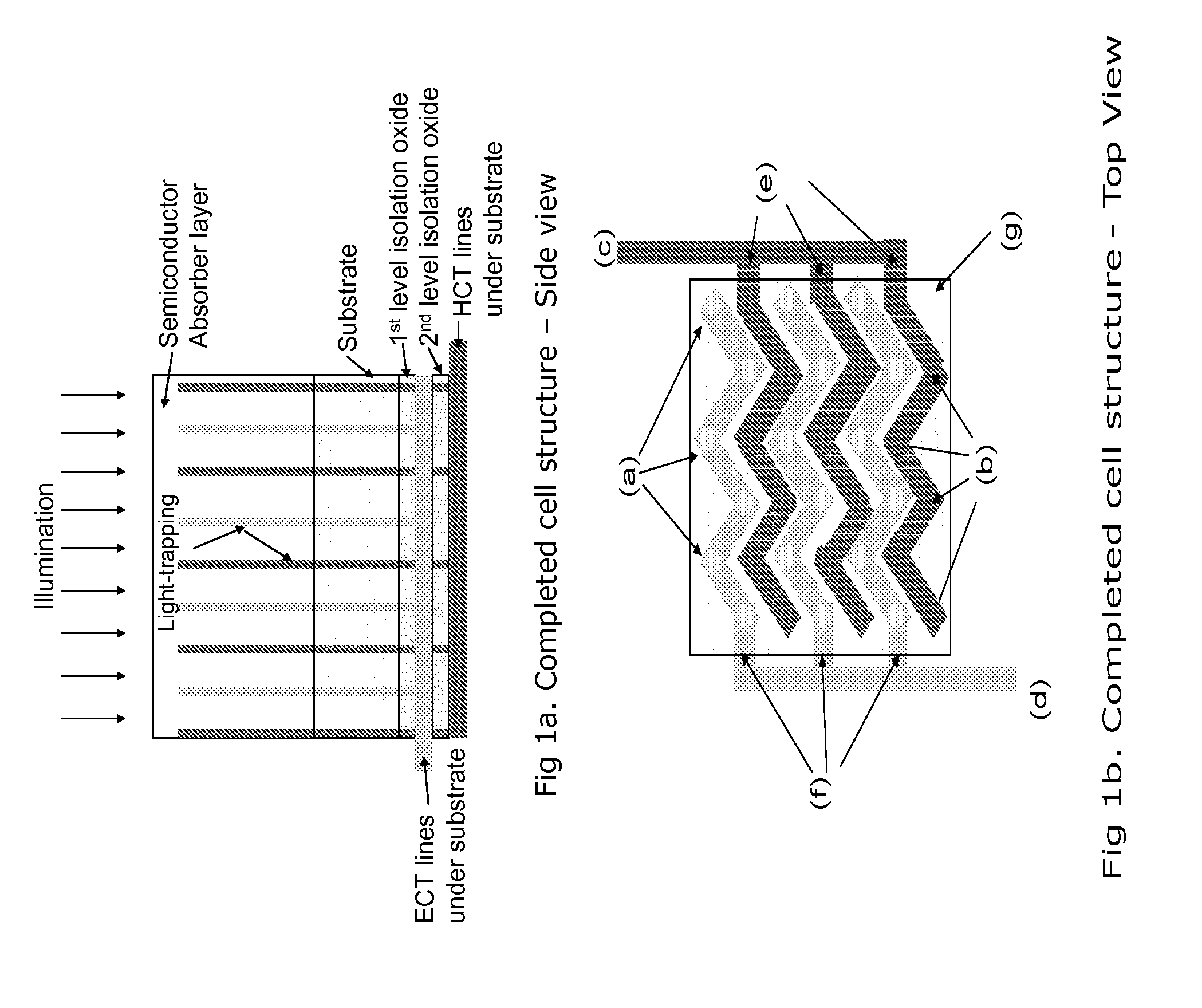
[0030]The problem described above is addressed through an innovative cell design which improves efficiency by 2 means: 1) enhanced light-trapping and 2) enhanced carrier collection. The basic cell design takes advantage of the simplicity of a Schottky junction as opposed to a more complex p-i-n diode.

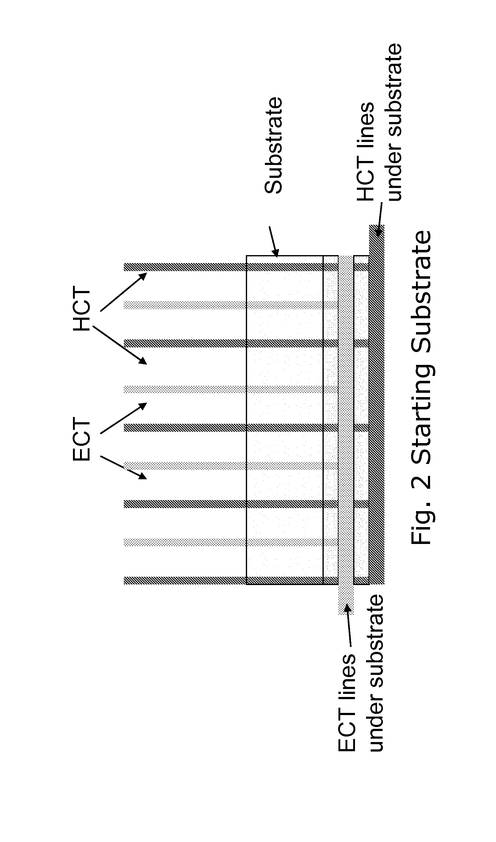
[0031]The preferred embodiment of the cell structure of this disclosure is shown in FIGS. 1a, 1b. It consists of a flexible substrate on which are fabricated contact pins in a pattern which alternates electron collection terminals (ECT) with hole collection terminals (HCT) such that each ECT is symmetrically surrounded by a number of HCTs and vice-versa, as shown in FIG. 2. The ECTs and HCTs are electrically isolated from each other at the substrate, while ...


PUM


Abstract

A Schottky contact photovoltaic energy conversion cell. The Schottky contact photovoltaic energy conversion cell comprises a flexible substrate and a first array of a plurality of closely-spaced microscale pillars connected to a first electrical cell contact. The pillars and the contact are formed of (or having a top) layer of a first Schottky metal material with a work function selected for efficiently collecting photogenerated electrons. The Schottky contact photovoltaic energy conversion cell further comprises a second array of a plurality of closely-spaced microscale pillars connected to a second electrical cell contact. The pillars and the contact are formed of (or having a top) layer of a second Schottky metal material with a work function selected for efficiently collecting photogenerated holes. The Schottky contact photovoltaic energy conversion cell further comprises a semiconductor absorber thin-film layer covering the first and second contacts and filling spaces among all the pillars, for creating photogenerated electrons and holes.

Description

[0001]This application claims the benefit of provisional patent application 60 / 823,200 filed on Aug. 22, 2006, which is hereby incorporated by reference.FIELD[0002]This disclosure relates in general to the field of solar cells, and more particularly to high efficiency solar cells and methods of manufacturing same.DESCRIPTION OF THE RELATED ART[0003]One of the key limitations to the wide-spread implementation of solar cells is their relatively low conversion efficiency (and another limitation is a relatively high manufacturing cost). As a result, the cost / watt of commercial photovoltaics is not competitive with fossil fuels and various conventional forms of grid-distributed electricity. There are a number of ways to increase cell efficiency through innovations in materials and cell designs. This disclosure discloses a specific thin-film solar cell and manufacturing method in order to mass produce high-efficiency, cost-reduced solar cells and modules.[0004]Large scale implementation o...

Claims


Application Information

Patent Timeline
Patent Type & Authority Applications(United States)
IPC IPC(8): H01L31/04H01L21/00
CPCH01L31/03529Y02E10/50H01L31/07
Inventor NAG, SOMNATHMOSLEHI, MEHRDAD
Owner BEAMREACH SOLAR INC
Why Eureka
Try Eureka