Charge pump pixel driving circuit

a technology of pixel driving circuit and charging pump, which is applied in the direction of instruments, static indicating devices, etc., can solve the problems of not meeting the demand of the current display device, and achieve the effect of maintaining the color performance of the display

Inactive Publication Date: 2008-03-06
IND TECH RES INST
View PDF7 Cites 29 Cited by
  • Summary
  • Abstract
  • Description
  • Claims
  • Application Information

AI Technical Summary

Benefits of technology

[0014]The above two types of charge pump pixel driving circuit can boost approximately twice or more times the data signal voltage provided to the pixel electrode. Moreover, the first storage capacitors of the above two types of charge pump pixel driving circuit can firstly store the sign

Problems solved by technology

And thus, the charge pump pixel driving circuit 100 of U.S. Pat. No. 5,903,248 is only applica

Method used


Image

  • Charge pump pixel driving circuit
  • Charge pump pixel driving circuit
  • Charge pump pixel driving circuit

Examples


Embodiment Construction

[0034]The charge pump pixel driving circuit of the present invention will be described in detail according to preferred embodiments accompanying with drawings.

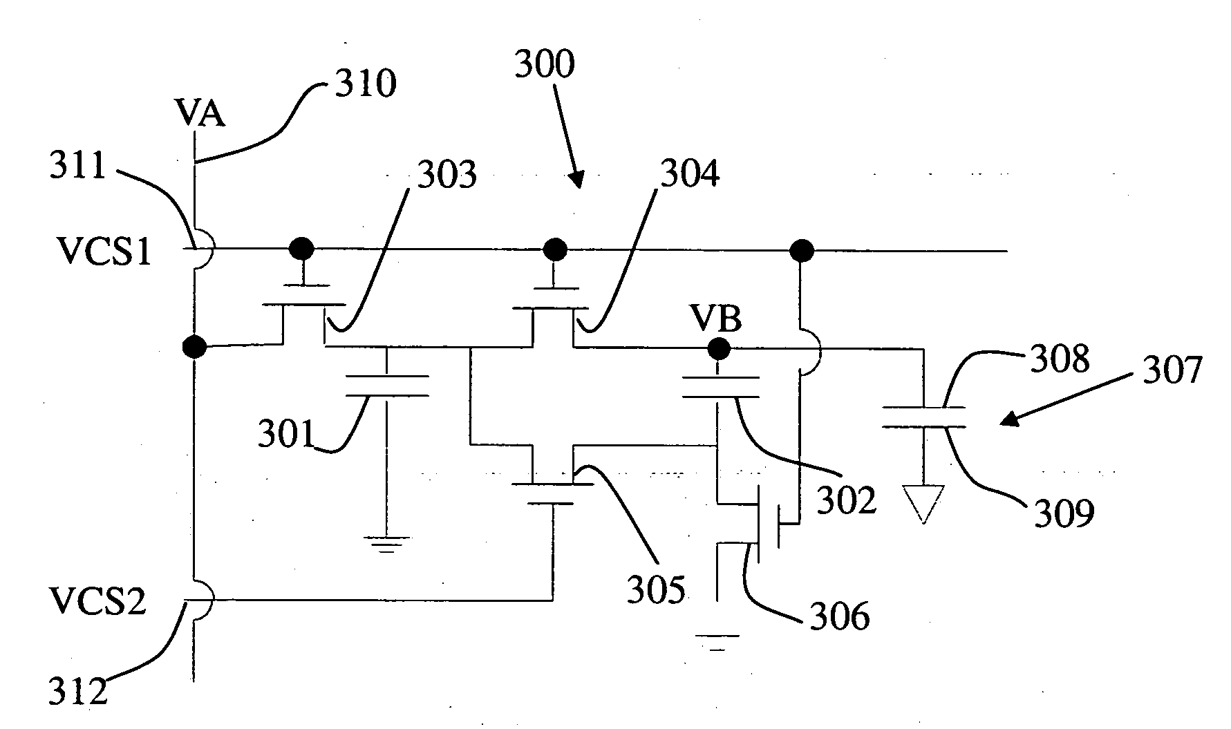
[0035]FIG. 3 is a schematic view of the charge pump pixel driving circuit in accordance with a first preferred embodiment of the present invention. In the first preferred embodiment, the charge pump pixel driving circuit 300 includes a first storage capacitor 301, a second storage capacitor 302 and a switch means having a first transistor 303, a second transistor 304, a third transistor 305 and a fourth transistor 306. The first transistor 303, the second transistor 304, the third transistor 305 and the fourth transistor 306 are N-channel transistors. A first end (high voltage end) of the first storage capacitor 301 is coupled to a source of the first transistor 303, and a second end (low voltage end) of the first storage capacitor 301 is grounded. A first end of the second storage capacitor 302 is coupled to a source of the s...


PUM


Abstract

The present invention provides a charge pump pixel driving circuit, which includes a first storage capacitor, a second storage capacitor and switch means. The first end of the second storage capacitor is coupled to a pixel electrode. The switch means responsive to a control signal to couple a signal voltage to the first ends of the first storage capacitor and second capacitor until the first ends of the first storage capacitor and second capacitor are charged to a voltage equal to the signal voltage. Then, the signal voltage is decoupled from the first storage capacitor and second storage capacitor, and the first end of the first storage capacitor is coupled to the second end of the second storage capacitor so that the first end of the second storage capacitor provides a voltage twice the signal voltage to the pixel electrode.

Description

BACKGROUND OF THE INVENTION[0001]1. Field of the Invention[0002]The present invention relates to a pixel driving circuit, and more particularly to a charge pump pixel driving circuit.[0003]2. Description of Related Art[0004]Charge pump is a circuit design for voltage multiplication, which can be employed in the pixel driving circuit of a display panel to design a charge pump pixel such that the data driving voltage can be boosted to twice or more times so as to eliminate power consumption or furthermore simplify the data driving circuit design.[0005]U.S. Pat. No. 5,903,248 provides a charge pump pixel driving circuit 100 applicable in the pixel driving circuit of the display device, as shown in FIG. 1. The charge pump pixel driving circuit 100 is used for driving a pixel 106 of an active matrix liquid crystal display device. The pixel 106 is constituted by a back plate electrode 110, a front plate electrode 111 and liquid crystal material 112 sandwiched between the two electrodes. T...

Claims


Application Information

Patent Timeline
IPC IPC(8): G09G3/36
CPCG09G3/3648G09G2300/0871G09G2300/0852G09G3/3659
Inventor CHEN, HENG-YINHUANG, JIH-FON
Owner IND TECH RES INST
Why Eureka
Try Eureka