Non-volatile semiconductor memory device

a semiconductor memory and non-volatile technology, applied in static storage, digital storage, instruments, etc., can solve the problems of reduced programming speed, reduced programming time, and wider threshold distribution of memory cells

Active Publication Date: 2008-03-06
KIOXIA CORP
View PDF9 Cites 18 Cited by
  • Summary
  • Abstract
  • Description
  • Claims
  • Application Information

AI Technical Summary

Benefits of technology

[0008]A non-volatile semiconductor memory device according to one embodiment of this invention comprises a plurality of word lines, and a plurality of bit lines comprising even numbered bit lines and odd numbered bit lines, and a memory cell array including a plurality of memory cells having two or more storage states, one of said plurality of memory cells being connected to a corresponding word line of said plurality of word lines, the number of storage states between adjacent memory cells is different in a word line direction and a bit line direction.
[0009]A non-volatile semiconductor memory device according to one embodiment of this invention comprises a plurality of word lines, and a plurality of bit lines comprising even numbered bit lines and odd numbered bit lines, and a memory cell array including a plurality of memory cells having two or more storage states, said plurality of memory cells having a first address and a second address, said second address being allocated and being the same between two said adjacent memory cells, one of said plurality of memory cells being connected to a corresponding word line of said plurality of word lines, the number of storage states between adjacent memory cells is different in a word line direction and a bit line direction, and a plurality of sense amplifiers connected to said plurality of bit lines, said sense amplifiers amplify and output a signal which is read from said plurality of memory cells, latches data which is input or output and converts said data based on said second address into a signal.
[0010]A non-volatile semiconductor memory device according to one embodiment of this invention comprises a plurality of word lines, and a plurality of bit lines comprising even numbered bit lines and odd numbered bit lines, and a memory cell array including a plurality of memory cells having two or more storage states, said plurality of memory cells having a first address, a second address and a third address, said second address being allocated and being the same between two said consecutive memory cells among three consecutive memory cells which are adjacent and said third address which is allocated to another memory cell among said three memory cells, one of said plurality of memory cells being connected to a corresponding word line of said plurality of word lines, the number of storage states of said memory cell among three consecutive memory cells which are adjacent is different, and a plurality of sense amplifiers connected to said plurality of bit lines, said sense amplifiers amplify and output a signal which is read from said plurality of memory cells, latches data which is input or output and converts said data based on said second address and said third address into a signal.

Problems solved by technology

However, by narrowing the step-up width of a programming voltage Vpgm, but then the threshold distribution of a memory cell becomes wider by the interference of an adjacent memory cell caused by capacitive coupling of the adjacent cell.
However, when narrowing the step-up width of a programming voltage Vpgm, the number of times the programming voltage Vpgm is applied increases, programming time becomes longer and programming speed is reduced.

Method used


Image

  • Non-volatile semiconductor memory device
  • Non-volatile semiconductor memory device
  • Non-volatile semiconductor memory device

Examples


embodiment one

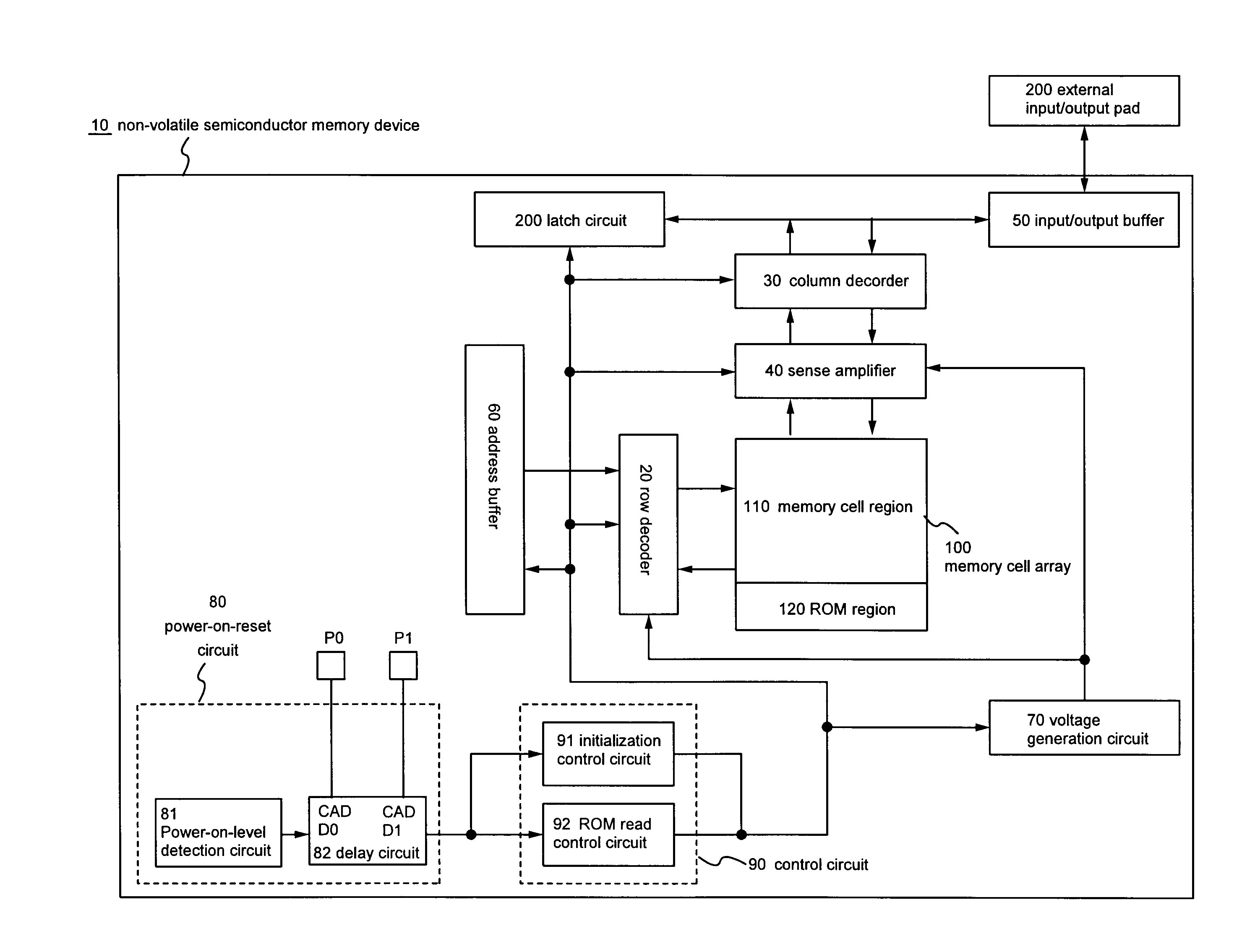
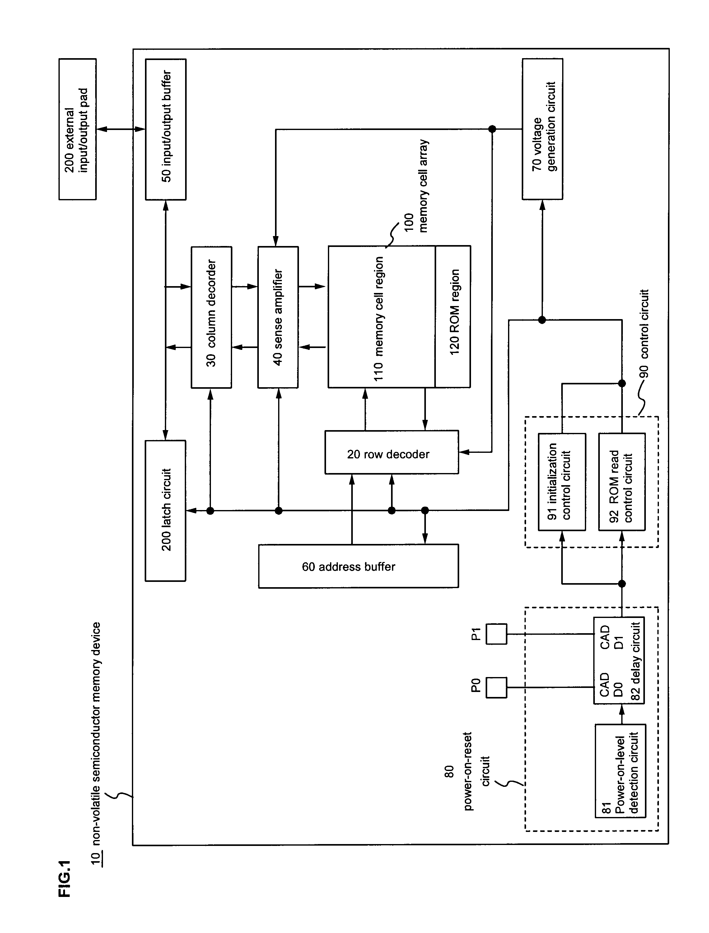
[0037]Below, the non-volatile semiconductor memory device relating to embodiment one of this invention will be explained in detail while referring to the drawings using a NAND type flash memory as an example. Further, an example of the non-volatile semiconductor memory device of this invention is shown in the embodiments, however, the non-volatile semiconductor memory device of this invention is not limited to these embodiments.

[0038]In a flash memory, by converting the amount of electric charge which is stored within a memory cell's floating gate electrode, that threshold is changed and data is stored. For example, (1) data corresponds to when the memory cell threshold is negative and (0) data corresponds to when it is positive.

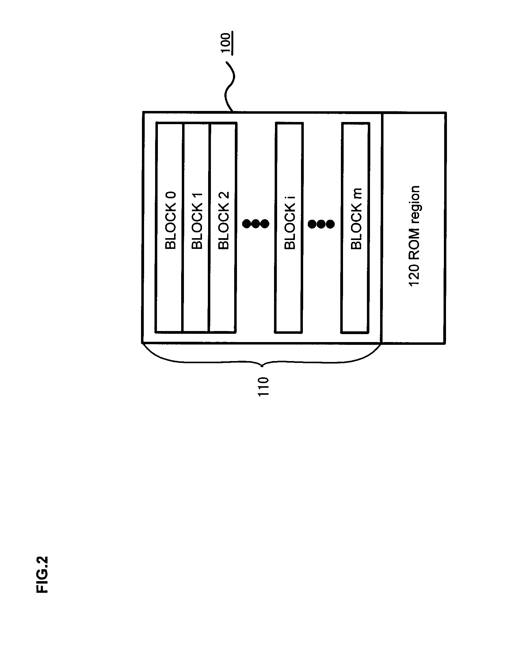
[0039]In recent years, in order to reduce the cost per unit of one data bit or to increase storage capacity, a plurality of data bits are stored in one cell, or what is called a multi-levels flash memory, is being developed. The threshold distribution of one...

embodiment two

[0137]In the non-volatile semiconductor memory device relating to embodiment two of the present invention, the operation mode allocation which is stored by a memory cell MC, is allocated into a checkered flag shape of two-levels data and eight-levels data.

[0138]In order to significantly increase storage capacity by memory chip high integration, further miniaturization than hitherto is required, however, it is possible to significantly increase storage capacity by storing multi data in one cell (data which has an amount of information of more than two-levels). In this case, a plurality of different threshold values are required for programming and reading and it is necessary to narrow the threshold distribution and the width of the step up. However, in the case of narrowing the threshold distribution, the effect of capacitive coupling with an adjacent memory cell becomes even greater and when storing data of an amount which has information of more than two-levels, because the number ...

embodiment three

[0151]In the case where data with an amount of information of more than two-levels is stored in a memory cell MC, the threshold distribution is narrowed by making the width of the step up of the program voltage smaller and a plurality of threshold distributions are inserted between a non selected read voltage and VSS. Therefore, the effect of capacitive coupling with an adjacent memory cell MC becomes larger by making a threshold voltage a high voltage by inserting a plurality of threshold distributions. In other words, the larger the amount of information in the data which is stored in a memory cell MC the higher the threshold voltage and thus the effect of capacitive coupling becomes larger.

[0152]In the non-volatile semiconductor memory device relating to one embodiment of the present invention, because an operation mode is allocated and controlled so that data which is stored in an adjacent memory cell MC in a word line direction and a bit line direction is made data with a diffe...


PUM


Abstract

A non-volatile semiconductor memory device includes plurality of word lines and a plurality of bit lines comprising even numbered bit lines and odd numbered bit lines and a memory cell array including a plurality of memory cells having two or more storage states, one of the plurality of memory cells being connected to a corresponding word line of the plurality of word lines, the number of storage states between adjacent memory cells is different in a word line direction and a bit line direction.

Description

CROSS REFERENCE TO RELATED APPLICATION[0001]This application is based upon and claims the benefit of priority from the prior Japanese Patent Applications No. 2006-239643, filed on Sep. 4, 2006; the entire contents of which are incorporated herein by reference.BACKGROUND OF THE INVENTION[0002]1. Field of the Invention[0003]This invention relates to a non-volatile semiconductor memory device and particularly, a NAND type flash memory.[0004]2. Description of the Related Art[0005]In recent years, in order to reduce the unit cost per one bit of data and increase storage capacity in a non-volatile semiconductor memory device such as a NAND type flash memory, a flash memory which stores multi-bit data, that is, a volume of information of more than two-levels of data, in one memory cell has been developed. Four threshold distributions of one memory cell in which two bits of data are stored exist corresponding to four-levels data.[0006]It is generally preferred that the form of the threshold...

Claims


Application Information

Patent Timeline
Patent Type & Authority Applications(United States)
IPC IPC(8): G11C16/04
CPCG11C11/5621G11C2211/5641G11C16/0483G11C11/5628
Inventor KANDA, KAZUSHIGE
Owner KIOXIA CORP
Why Eureka
Try Eureka