STRUCTURES AND METHODS FOR MANUFACTURING OF DISLOCATION FREE STRESSED CHANNELS IN BULK SILICON AND SOI MOS DEVICES BY GATE STRESS ENGINEERING WITH SiGe AND/OR Si:C

a technology of gate stress engineering and mos, which is applied in the direction of semiconductor devices, electrical equipment, basic electric elements, etc., can solve the problems of crystal structure dislocation and crystal structure dislocation caused by strong strain, and achieve the effect of controlling the stress in the channels of the devi

Inactive Publication Date: 2008-03-13
GLOBALFOUNDRIES INC
View PDF16 Cites 14 Cited by
  • Summary
  • Abstract
  • Description
  • Claims
  • Application Information

AI Technical Summary

Benefits of technology

[0008] avoids dislocations generated in channels of bulk silicon and SOI (silicon on insulator) MOS (metal oxide semiconductor) devices;
[0012] overcomes problems associated with the requirement that high Ge % SSi / SiGe require the SSi to be very thin in order to reduce the generation of dislocations. However, if the strained Si is too thin, (e.g. 5 nm, corresponding to 35% Ge critical thickness), the interface of SSi / SiGe can degrade mobility.
[0015] allows the use of large Ge % and thickness of SiGe to produce large stresses due to the interfaces of SSi / SiGe or SSi / Si:C in the gates;
[0017] controls the stress in the channels of the devices by tuning Ge % or C % in SiGe or Si:C or by changing the thickness of the films;

Problems solved by technology

Moreover, strong strain often creates dislocations in crystal structures.

Method used


Image

  • STRUCTURES AND METHODS FOR MANUFACTURING OF DISLOCATION FREE STRESSED CHANNELS IN BULK SILICON AND SOI MOS DEVICES BY GATE STRESS ENGINEERING WITH SiGe AND/OR Si:C
  • STRUCTURES AND METHODS FOR MANUFACTURING OF DISLOCATION FREE STRESSED CHANNELS IN BULK SILICON AND SOI MOS DEVICES BY GATE STRESS ENGINEERING WITH SiGe AND/OR Si:C
  • STRUCTURES AND METHODS FOR MANUFACTURING OF DISLOCATION FREE STRESSED CHANNELS IN BULK SILICON AND SOI MOS DEVICES BY GATE STRESS ENGINEERING WITH SiGe AND/OR Si:C

Examples


Embodiment Construction

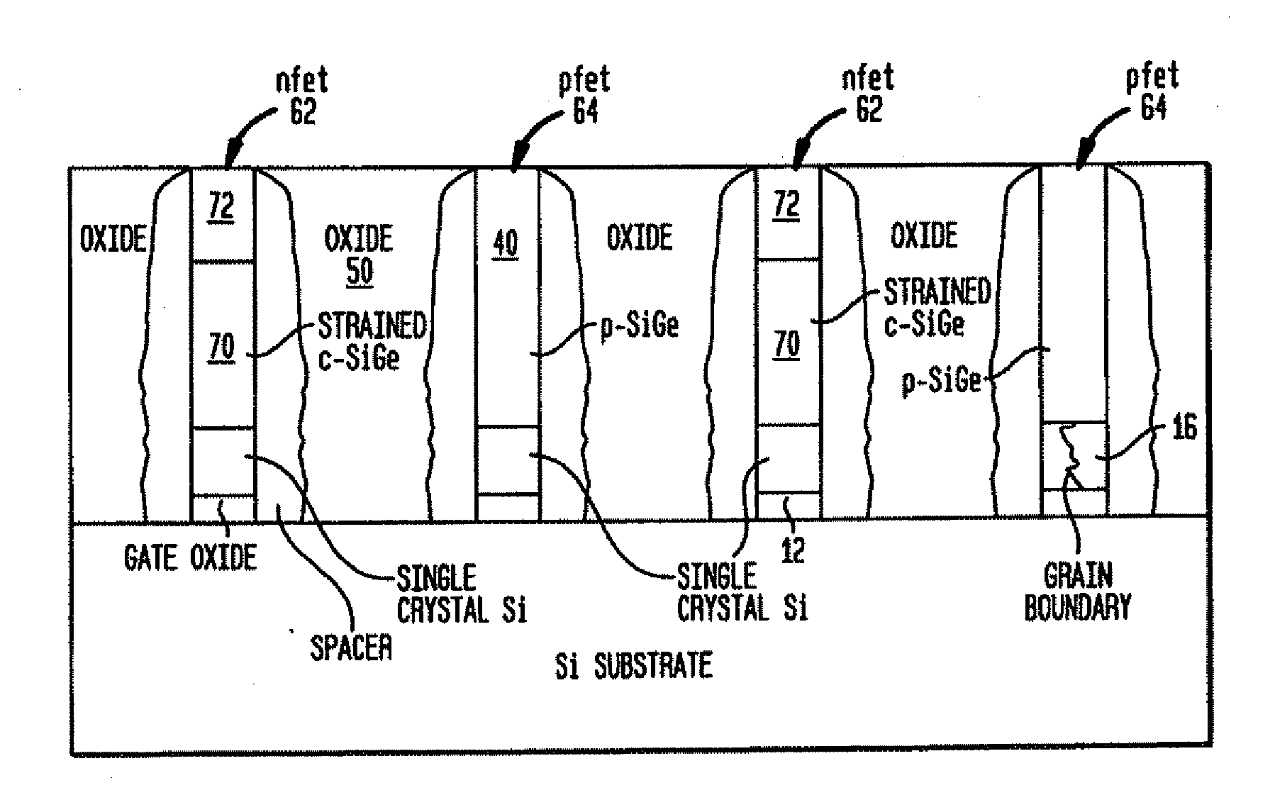
[0040]FIGS. 1 through 8 illustrate the fabrication process steps of a first embodiment of the present invention.

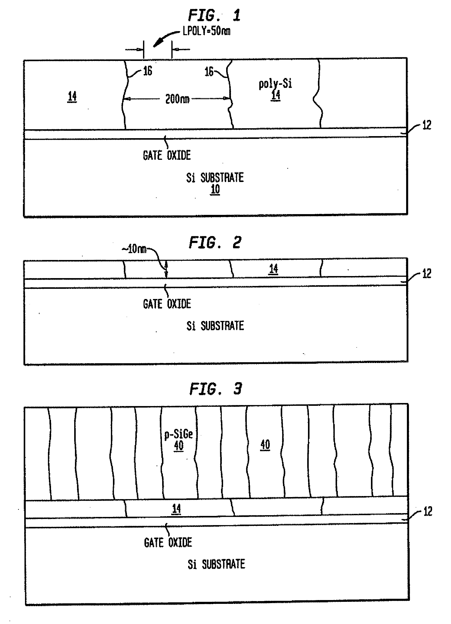
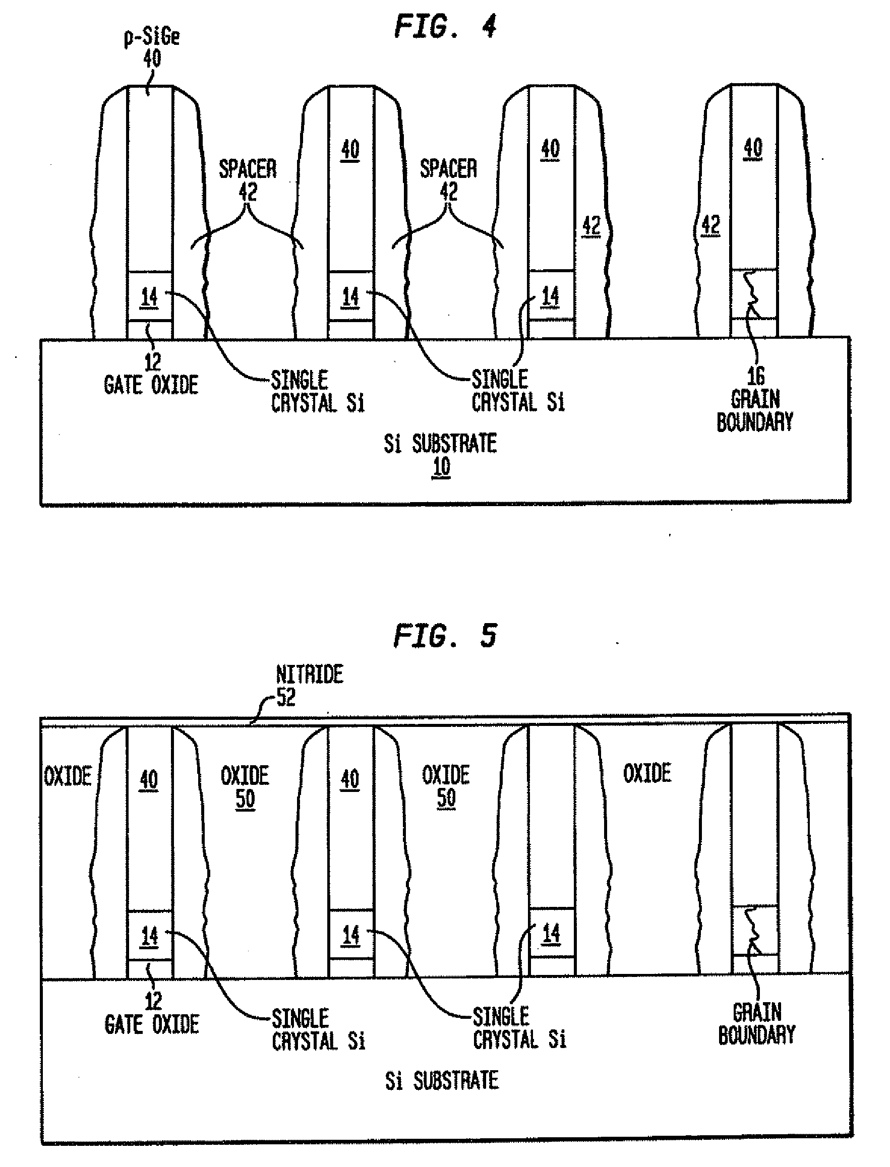
[0041]FIG. 1 illustrates the structure after the completion of steps 1 and 2. Step 1 uses conventional processes to form a gate oxide 12 on a Si substrate 10 (alternate embodiments can employ an SOI technology) of a wafer, and step 2 involves depositing a-Si (amorphous silicon) or poly-Si, and annealing the a-Si or poly-Si to obtain poly-Si 14 with a large grain size. If the grain size is approximately 200 nm, as shown in FIG. 1, for a 50 nm gate device (shown as Lpoly=50 nm), there is a 75% probability of not seeing a grain boundary 16 in the lateral direction of the gate, as illustrated by FIG. 1. The grain boundaries assist in relieving stress in the material.

[0042]FIG. 2 illustrates the structure after step 3 involving oxidation and etching the oxide on the large grain poly-Si layer until reaching ˜10 nm thickness.

[0043]FIG. 3 illustrates the structure after step 4 ...


PUM

PropertyMeasurementUnit
thicknessaaaaaaaaaa
thicknessaaaaaaaaaa
grain sizeaaaaaaaaaa

Abstract

Structures and methods of manufacturing are disclosed of dislocation free stressed channels in bulk silicon and SOI (silicon on insulator) CMOS (complementary metal oxide semiconductor) devices by gate stress engineering with SiGe and / or Si:C. A CMOS device comprises a substrate of either bulk Si or SOI, a gate dielectric layer over the substrate, and a stacked gate structure of SiGe and / or Si:C having stresses produced at the interfaces of SSi(strained Si) / SiGe or SSi / Si:C in the stacked gate structure. The stacked gate structure has a first stressed film layer of large grain size Si or SiGe over the gate dielectric layer, a second stressed film layer of strained SiGe or strained Si:C over the first stressed film layer, and a semiconductor or conductor such as p(poly)-Si over the second stressed film layer.

Description

RELATED APPLICATIONS [0001] This application is a divisional application of U.S. Ser. No. 10 / 709,239, filed Apr. 23, 2004.BACKGROUND OF THE INVENTION [0002] 1. Field of the Invention [0003] The present invention relates generally to structures and methods of manufacturing dislocation free stressed channels in bulk silicon and SOI (silicon on insulator) MOS (metal oxide semiconductor) devices by gate stress engineering with SiGe and / or Si:C. [0004] Dislocations are defects in crystal structures, and disadvantageously can provide current paths for leakage currents in bulk silicon and SOI CMOS devices having such dislocations. SUMMARY OF THE INVENTION [0005] The present invention provides structures and methods of manufacturing dislocation free stressed channels in bulk Si and SOI MOS (metal oxide semiconductor) devices by gate stress engineering with SiGe and / or Si:C. A MOS device comprises a substrate of either bulk Si or SOI, a gate dielectric layer over the substrate, and a stacked...

Claims


Application Information

Patent Timeline
Patent Type & Authority Applications(United States)
IPC IPC(8): H01L21/3205H01L21/20H01L21/28H01L21/8238H01L21/84H01L27/12H01L29/49H01L29/78H01L31/0392
CPCH01L21/28035H01L21/823807H01L21/823828H01L21/84H01L29/7845H01L29/4925H01L29/66545H01L29/7842H01L27/1203
Inventor ZHU, HUILONGDORIS, BRUCE B.CHEN, HUAJIE
Owner GLOBALFOUNDRIES INC
Why Eureka
Try Eureka