Eureka AIR delivers breakthrough ideas for toughest innovation challenges, trusted by R&D personnel around the world.

Heterogeneous integration of low noise amplifiers with power amplifiers or switches

a technology of power amplifier or switch and low-noise amplifier, which is applied in the direction of transistors, electrical devices, semiconductor devices, etc., can solve the problems of sacrificing the low-noise characteristics of low-noise amplifiers, unable to optimize simultaneously with one another on the same substrate, and using a phemt is a lower breakdown voltag

Inactive Publication Date: 2008-03-20
TELEDYNE SCI & IMAGING
View PDF10 Cites 2 Cited by
  • Summary
  • Abstract
  • Description
  • Claims
  • Application Information

AI Technical Summary

Benefits of technology

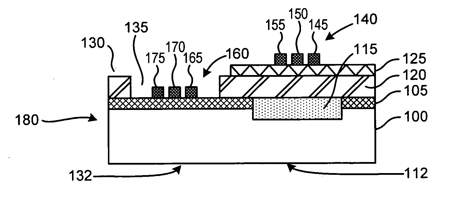
[0019]One embodiment of the invention includes a transistor heterogeneously integrating a power amplifier or switch with a low-noise amplifier having a substrate wafer suitable for high electron mobility transistors. The substrate wafer has a first end and a second end, a conducting layer above the first end of the substrate wafer, an isolation implant that renders the conducting layer insulating, a buffer layer deposited above the conducting layer and configured for the low-noise amplifier, and an active layer deposited above the second end of the substrate wafer and configured for the low-noise amplifier.
[0020]In one embodiment, the substrate wafer can be Gallium Arsenide (GaAs), Indium Phosphide (InP) or Gallium Antimonide (GaSb). The active layer can include a layer of Indium Arsenide (InAs) and / or a layer of Aluminum Antimonide (AlSb). In addition, the conducting layer may be a pseudomorphic high electron mobility layer such as an active Gallium Arsenide (GaAs) layer.
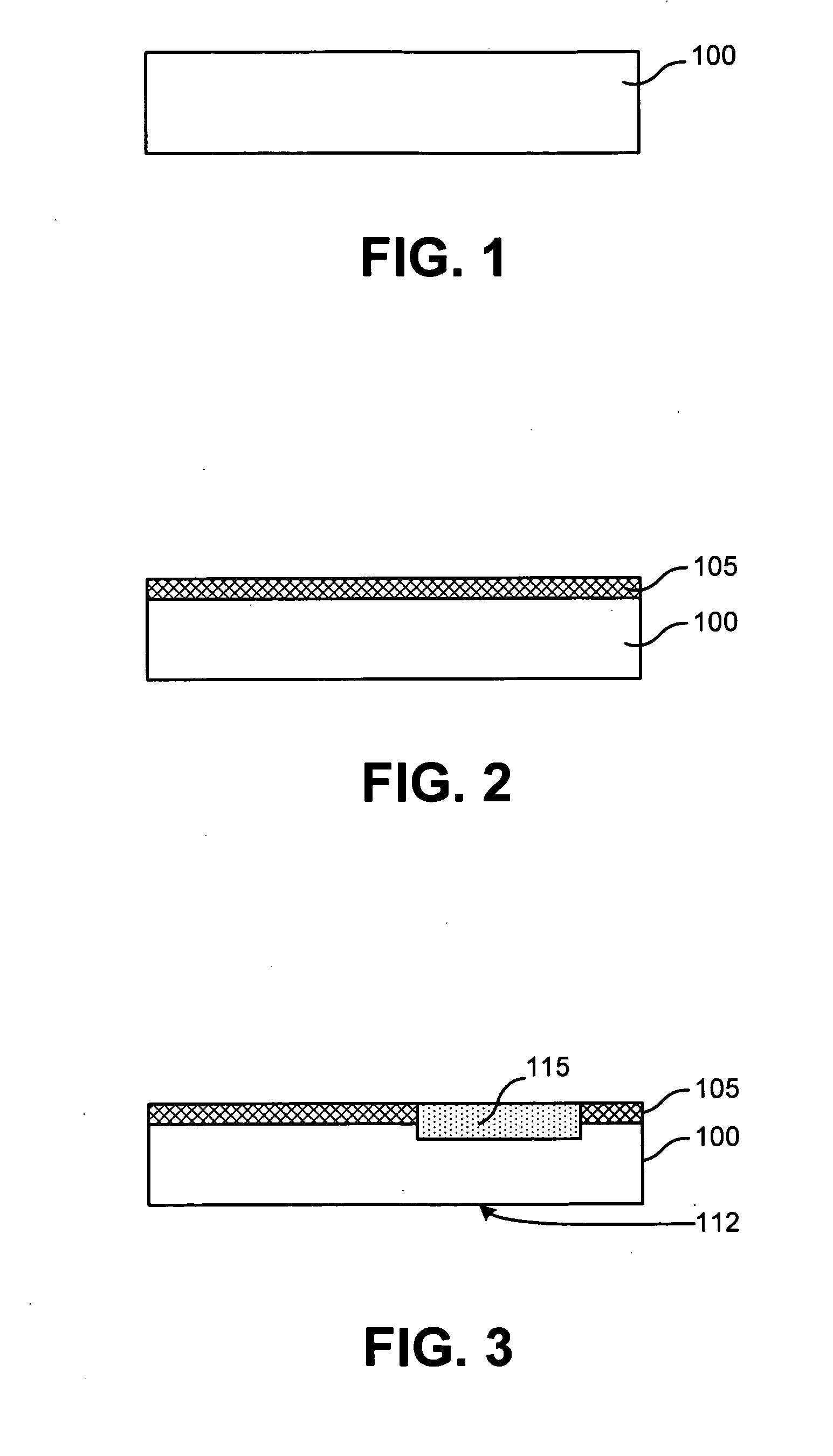
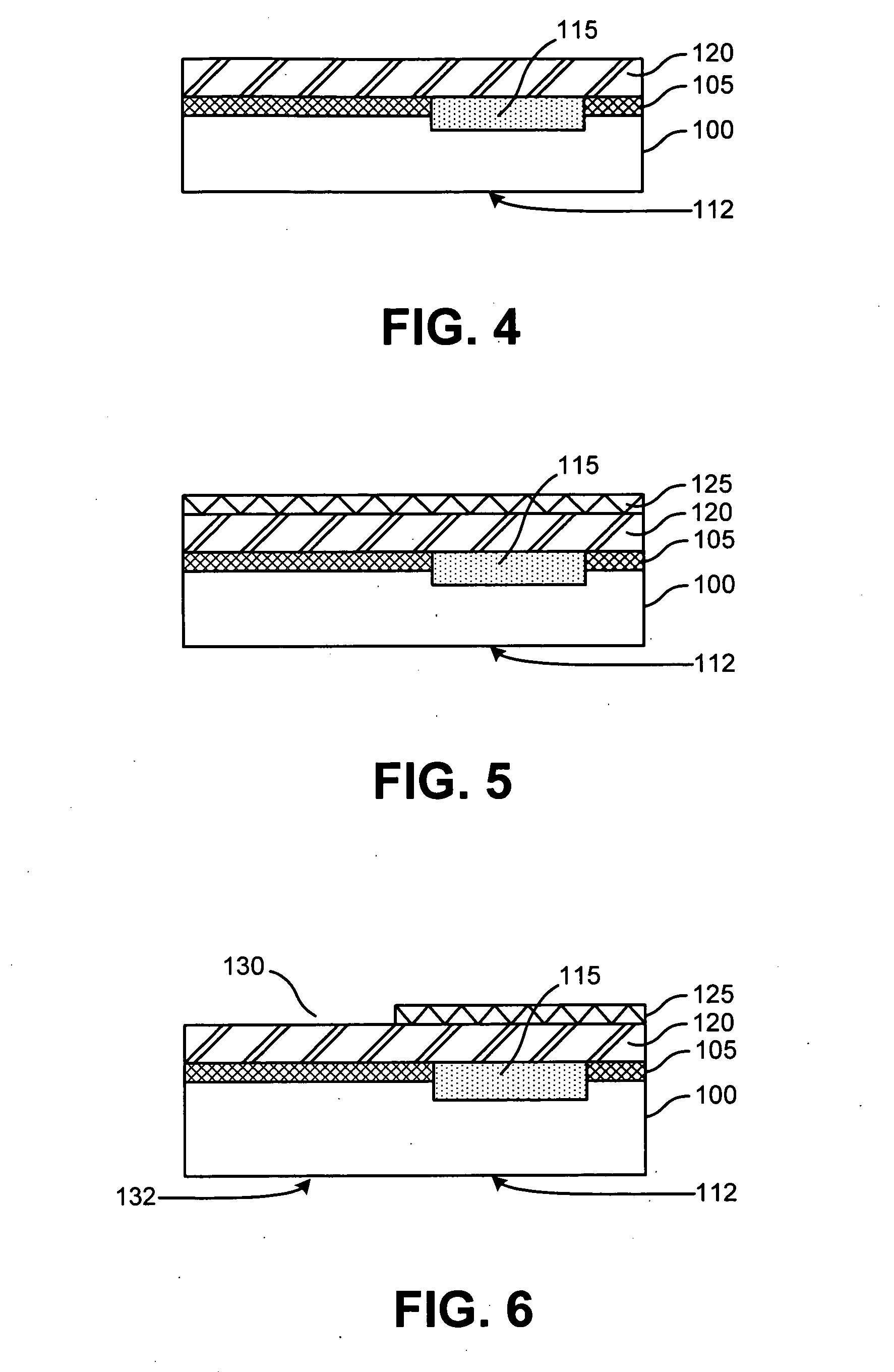
[0021]The method for heterogeneously integrating the power amplifier or switch with the low-noise amplifier includes depositing conducting layer above a substrate wafer suitable for high electron mobility transistors, implanting ions in a first end of the conducting layer, depositing a first active layer above the first end of the conducting layer and configured for the low-noise amplifier, and depositing metal contacts for the low-noise amplifier at the first end of the conducting layer and for the power amplifier or switch at a second end of the conducting layer.

Problems solved by technology

However, the disadvantage of using a PHEMT is a lower breakdown voltage when the concentration of Indium (In) is greater than the amount required for lattice matching to the substrate or barrier.
While prior art transistors can be optimized for either a low-noise amplifier for receivers or a power amplifier for transmitters, they cannot be optimized simultaneously with one another on the same substrate.
This is because the low-noise amplifier cannot withstand large voltages used for the power amplifier without sacrificing its low noise characteristics.

Method used


Image

  • Heterogeneous integration of low noise amplifiers with power amplifiers or switches
  • Heterogeneous integration of low noise amplifiers with power amplifiers or switches
  • Heterogeneous integration of low noise amplifiers with power amplifiers or switches

Examples


Embodiment Construction

[0022]Methods and systems that implement the embodiments of the various features of the invention will now be described with reference to the drawings. The drawings and the associated descriptions are provided to illustrate embodiments of the invention and not to limit the scope of the invention. Reference in the specification to “one embodiment” or “an embodiment” is intended to indicate that a particular feature, structure, or characteristic described in connection with the embodiment is included in at least an embodiment of the invention. The appearances of the phrase “in one embodiment” or “an embodiment” in various places in the specification are not necessarily all referring to the same embodiment. Throughout the drawings, reference numbers are re-used to indicate correspondence between referenced elements.

[0023]Prior art transistors are typically used for either a low-noise amplifier for receivers or a power amplifier for transmitters. Low-noise amplifiers and power amplifier...


PUM


Abstract

A transistor heterogeneously integrating a power amplifier or switch with a low-noise amplifier having a substrate wafer selected from a group consisting of Gallium Arsenide (GaAs), Indium Phosphate (InP) and Gallium Antimonide (GaSb), the substrate wafer having a first end and a second end, a conducting layer above the first end of the substrate wafer, an isolation implant providing lateral isolation in the conducting layer, a first active layer deposited above the conducting layer and configured for the low-noise amplifier, and a buffer layer deposited above the conducting layer and configured for the low-noise amplifier.

Description

BACKGROUND OF THE INVENTION[0001]1. Field of the Invention[0002]The invention relates generally to High Electron Mobility Transistors (HEMTs). More particularly, the invention relates to a heterogeneous integration of low noise HEMT amplifiers with Pseudomorphic HEMT (PHEMT) power amplifiers or switches.[0003]2. Description of Related Art[0004]When donors are placed in a material with a higher conduction band energy than the channel, and close to the channel, they create an electron gas with high electron mobility in the channel. Transistors that implement this concept are known in the art as High Electron Mobility Transistors (HEMT).[0005]Most HEMTs require at least two materials: barrier and channel materials. The barrier material that contains the donor must have a higher conduction band energy, but also improves the device breakdown by having a wider bandgap to accommodate high fields. The channel material that makes up the conducting layer is selected based on the transport pro...

Claims


Application Information

Patent Timeline
Patent Type & Authority Applications(United States)
IPC IPC(8): H01L29/80
CPCH01L27/0605
Inventor BRAR, BERINDERBERGMAN, JOSHUA I.IKHLASSI, AMALNAGY, GABORSULLIVAN, GERARD J.
Owner TELEDYNE SCI & IMAGING
Why Eureka
Eureka Blog
Learn More