High density photodiodes

a photodiode and high density technology, applied in the field of radiological detectors, can solve the problems of negating the benefits of the smaller device size, difficult to provide efficient interconnection between devices, and inconvenient cost, and achieve the effects of high density photocurrent, low cost, and uniformity

a photodiode and high density technology, applied in the field of radiological detectors, can solve the problems of negating the benefits of the smaller device size, difficult to provide efficient interconnection between devices, and inconvenient cost, and achieve the effects of high density photocurrent, low cost, and uniformity

US20080067622A1Inactive Publication Date: 2008-03-20OSI OPTOELECTRONICS

Image

  • High density photodiodes
  • High density photodiodes
  • High density photodiodes

Examples


Embodiment Construction

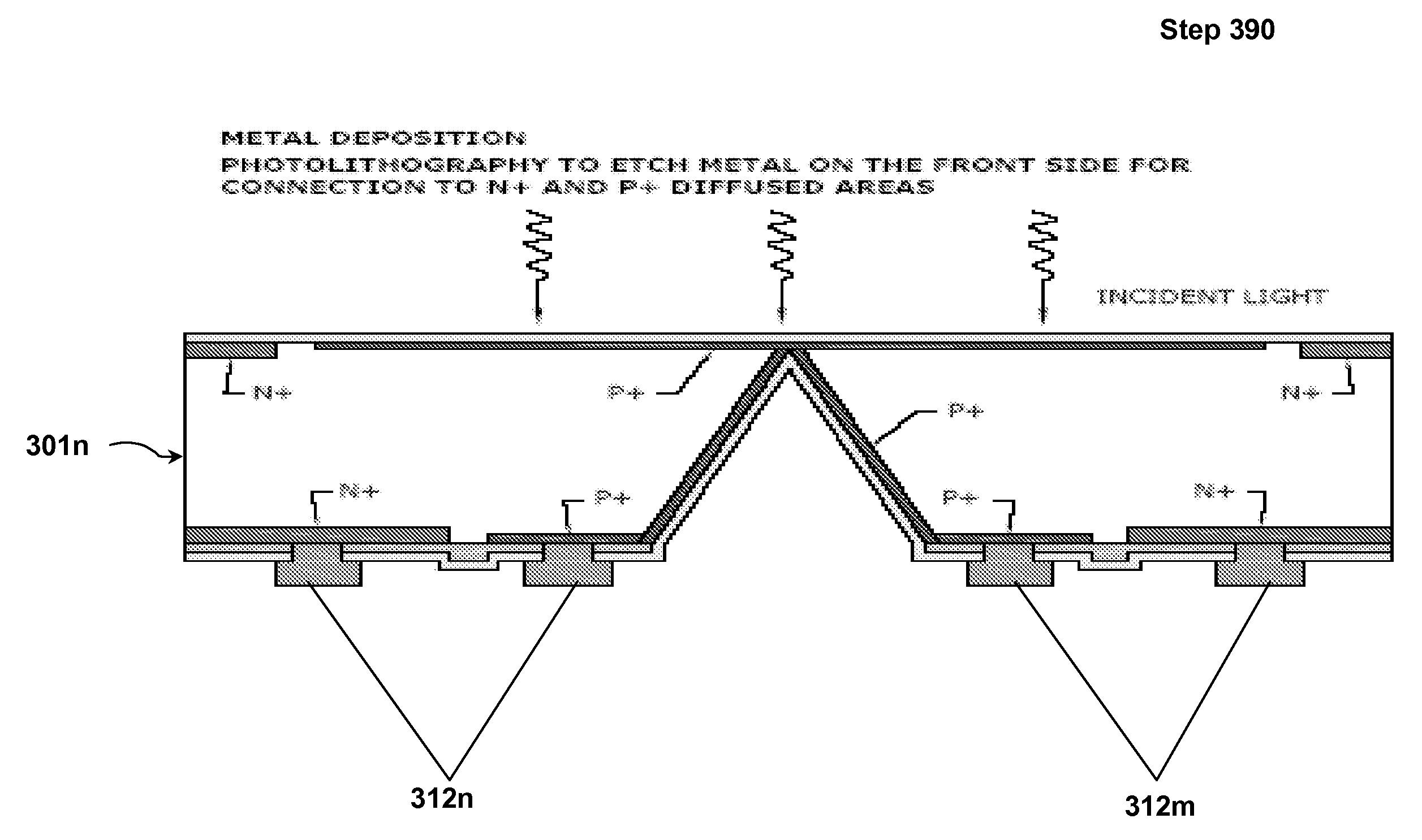
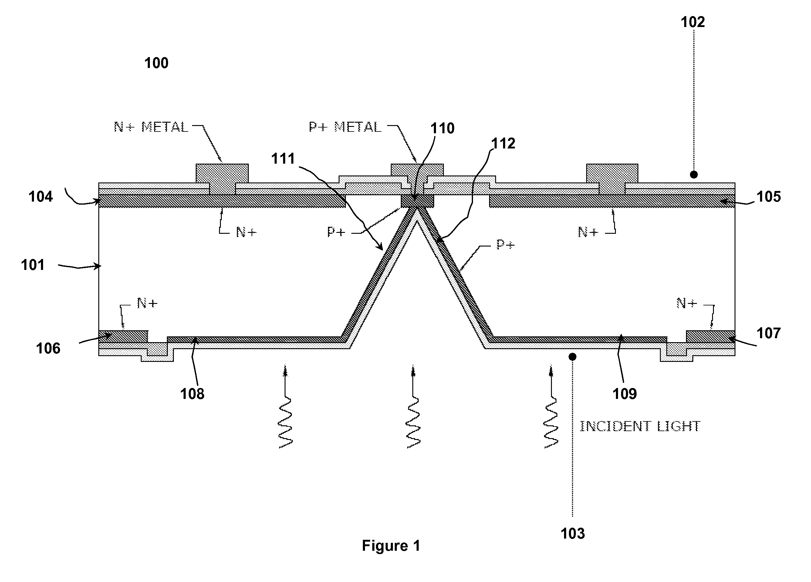
[0027]The present invention is directed towards detector structures, detector arrays, and design and implementation of detector arrays for an assortment of applications including, but not limited to, computerized tomography (CT) and non-CT applications. Specifically, the present invention is directed towards high-density photodiode arrays manufactured at high-throughput and low-cost, capable of generating uniform as well as high density photocurrent.

[0028]More specifically, the present invention is directed towards a front-side contact, back-side illuminated (FSC-BSL) photodiode array having improved characteristics, including high production throughput, low-cost manufacturing via implementation of batch processing techniques; uniform as well as high photocurrent density owing to presence of a large continuous homogeneous, heavily doped layer; and back to front intrachip connections via the homogenous, heavily doped layers on the front and back sides of the substrate.

[0029]In one em...


PUM


Abstract

The present invention is a front-side contact, back-side illuminated (FSC-BSL) photodiode arrays and front-side illuminated, back-side contact (FSL-BSC) photodiode arrays having improved characteristics, including high production throughput, low-cost manufacturing via implementation of batch processing techniques; uniform, as well as high, photocurrent density owing to presence of a large continuous homogeneous, heavily doped layer; and back to front intrachip connections via the homogenous, heavily doped layers on the front and back sides of the substrate.

Description

FIELD OF THE INVENTION[0001]The present invention relates generally to the field of radiation detectors, and in particular, relates to front-side contact, back-side illuminated (FSC-BSL) photodiode arrays and front-side illuminated, back side contact (FSL-BSC) photodiode arrays having a plurality of heavily doped n+ and p+ diffused regions and further comprising three-dimensional (3D)-microstructures, such as grooves, pits, and cavities for forming electrical connections. Still more particularly, the present invention relates generally to photodiode arrays that can be manufactured with high-throughput and low cost and that are capable of generating a uniform, high-density photocurrent.BACKGROUND OF THE INVENTION[0002]Photodiode arrays or photodiodes are used in an assortment of applications including, but not limited to, radiation detection, optical position encoding, and low light-level imaging, such as night photography, nuclear medical imaging, photon medical imaging, multi-slice...

Claims


Application Information

Patent Timeline
20 Mar 2008
Publication
US20080067622A1
IPC
H01L31/00; H01L29/76
CPC
H01L27/1446; H01L27/14683; H01L27/14692; H01L31/02016; Y02E10/50; H01L31/035281; H01L31/03529; H01L31/105
Inventors
BUI, PETER STEVEN; TANEJA, NARAYAN DASS