LED Including Photonic Crystal Structure

a technology of photonic crystal structure and led, which is applied in the direction of basic electric elements, electrical apparatus, and semiconductor devices, can solve the problems of poor extraction efficiency, less than 30%, and limited extraction efficiency, and achieve the effect of improving the performance and reliability of pxled and low defect density

Inactive Publication Date: 2008-03-20
LUMILEDS
View PDF26 Cites 17 Cited by
  • Summary
  • Abstract
  • Description
  • Claims
  • Application Information

AI Technical Summary

Benefits of technology

[0017] The parameters characterizing the lattice of the holes, include the lattice constant, the diameter of the holes, the depth of the holes, and the dielectric constant of the dielectric in the holes. In some embodiments these parameters are chosen such that the wavelength of the emitted light lies close to the edge of the energy bands of the photonic crystal, because close to the band edge the density of states of the photons is large. The recombination energy can be emitted much more efficiently through photons with a large density of states. Therefore, in embodiments of the present invention that emit light with energies close to the band edge, the emitted power can exceed the power emitted by the same LED without the periodic structure up to about eight times. This enhancement can be related to the presence of metal electrode layers in embodiments of the invention that enhance the efficiency and increase the emitted power of the PXLEDs.
[0018] The present embodiments are formed from III-Nitride compounds, which include Nitrogen and a group III element, such as Gallium, Aluminum, or Indium. III-Nitride compounds are used because their surface recombination velocities are more than ten times smaller than that of GaAs, according to M. Boroditsky et al., in J. App. Phys. vol. 87, p. 3497 (2000). As described above, a low surface recombination velocity can increase the efficiency of a PXLED above the efficiency of a regular LED without the photonic crystal structure, making GaN PXLEDs technically and economically viable candidates for improved light generation efficiency.
[0019] Additionally, GaN LEDs are the leading candidates for generating light in the blue and green regime of the spectrum; therefore, increasing their efficiency is highly desired. Finally, since the external quantum efficiency of GaN LEDs is often in the vicinity of 10 percent, the formation of photonic crystals can improve the efficiency of a GaN LED in a substantial manner. Here the external quantum efficiency is the product of the internal quantum efficiency and the extraction efficiency.
[0021] Some methods of the invention create a PXLED by forming a patterned masking layer with openings on a substrate. Then the epitaxial lateral overgrowth technique (“ELOG”) is used to form an n-doped layer overlying the masking layer, an active layer overlying the n-doped layer, a p-doped layer overlying the active layer, and a p-electrode layer on the p-doped layer. The ELOG technique creates semiconductor layers with a low density of defects, improving the performance and reliability of the PXLEDs. A second substrate is formed on the electrode layer and the first substrate is removed to expose the masking layer. Next, the semiconductor layers are at least partially removed through the openings of the masking layer to form a lattice of holes. Finally, the masking layer is used as the p-electrode layer, and an n-electrode layer is formed on the n-doped layer.

Problems solved by technology

The extraction efficiency is limited, among others, by the emitted photons suffering multiple total internal reflections at the walls of the high refractive index semiconductor medium.
As a result, the emitted photons do not escape into free space, leading to poor extraction efficiencies, typically less than 30%.
However, none of these geometries can entirely eliminate losses from total reflection.
A further source of loss is the reflection caused by the refractive index mismatch between the LED and the surrounding media.
However, the device of U.S. Pat. No. 5,955,749 is not operational and therefore is not a LED.
However, for PXLEDs, neither the fabrication of electrodes, nor their influence on the operation of the PXLED is obvious.
Also, electrodes are typically thought to reduce the extraction efficiency as they reflect a portion of the emitted photons back into the LED, and absorb another portion of the emitted light.
However, when electrons and holes recombine through intermediate electronic states in the gap, then the recombination energy is emitted in the form of heat instead of photons, reducing the light emission efficiency of the LED.
However, on the surface of semiconductors typically there are a large number of surface states and defect states, many of them in the gap.
This surface recombination generates heat instead of light, considerably reducing the efficiency of the LED.
However, PXLEDs include a large number of holes, thus PXLEDs have a much larger surface area than the regular LEDs.
Therefore, the surface recombination may be capable of reducing the efficiency of the PXLED below the efficiency of the same LED without the photonic crystal structure, making the formation of photonic crystal structure pointless.
Since GaAs has a high surface recombination velocity, it is not a promising candidate for fabricating photonic crystal LEDs.
In particular, U.S. Pat. No. 5,955,749 does not describe the successful operation of a photonic crystal LED.
Also, U.S. Pat. No. 5,955,749 does not describe the influence of the photonic crystal on the emission process, which can affect the internal efficiency of the LED.
While photonic crystals are promising for light extraction for the reasons described above, there are problems with the design.
However, Lee et al. do not show how to form and operate a light emitting device with this design.
The addition of the electrodes, however, will substantially affect the extraction and the spontaneous emission.
Since this effect is unknown, it cannot be disregarded in the design of a LED.

Method used


Image

  • LED Including Photonic Crystal Structure
  • LED Including Photonic Crystal Structure
  • LED Including Photonic Crystal Structure

Examples


Embodiment Construction

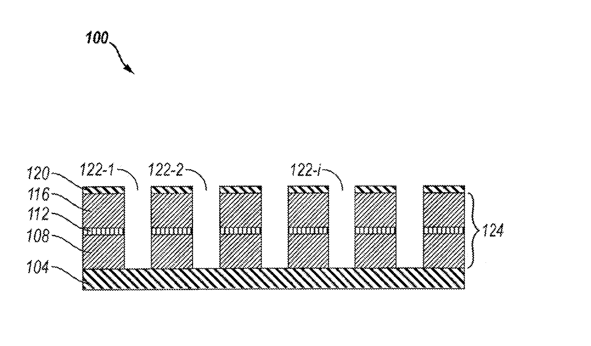
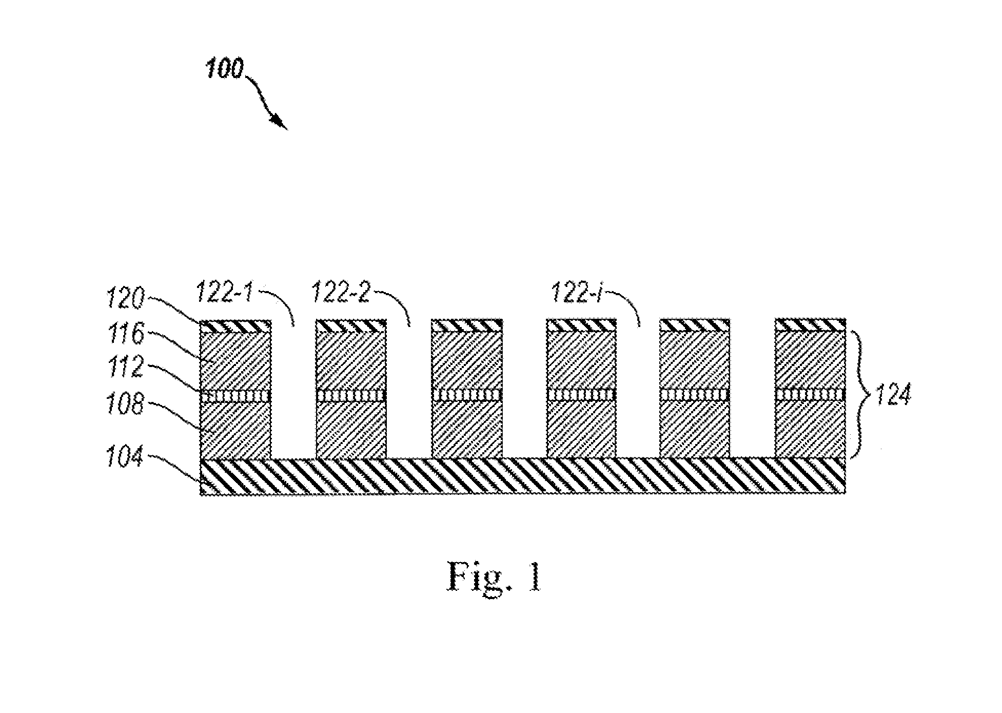
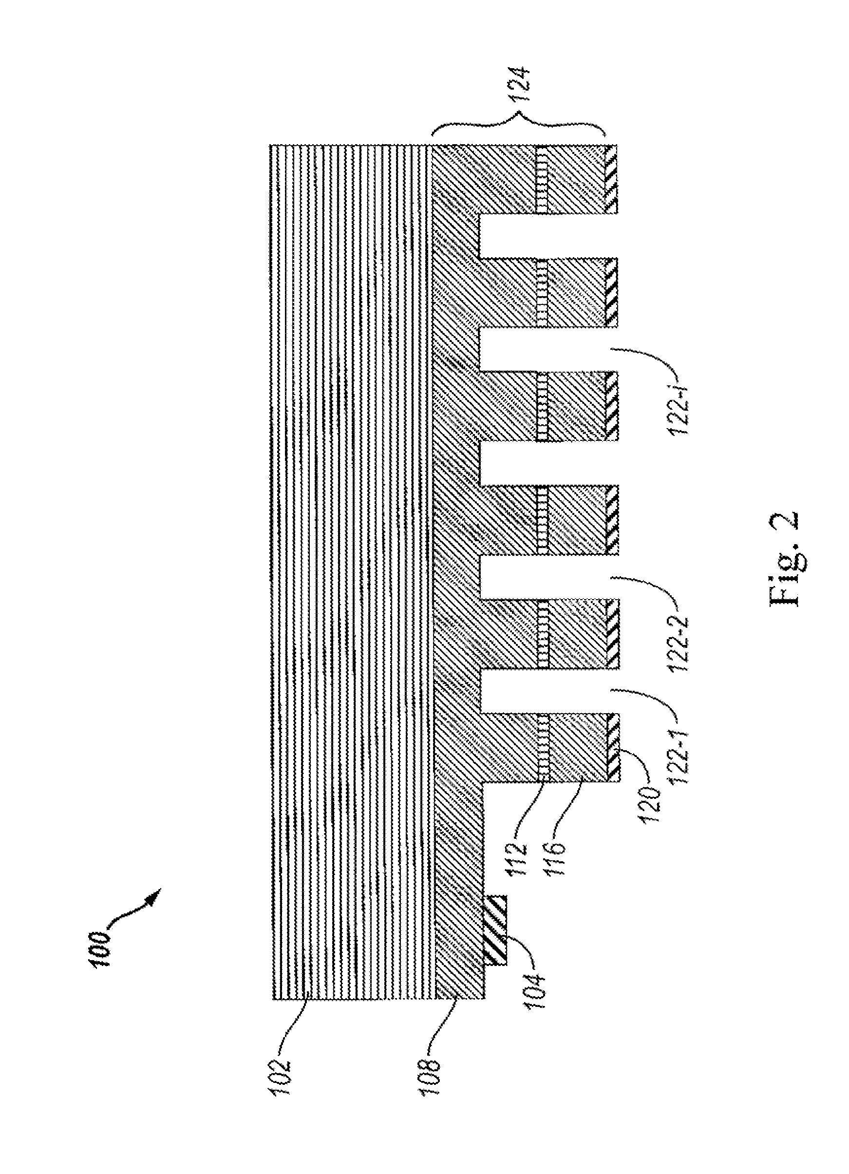
[0037]FIG. 1 illustrates an embodiment of a photonic crystal LED (“PXLED”) 100. A first electrode layer 104 is formed from a thick and substantially reflective metal. In some embodiments first electrode layer 104 also serves as a substrate. In some embodiments first electrode layer 104 can overlie a substrate. Many different metals can be used for forming first electrode layer 104, including Au, Al, Ag, and heavily doped semiconductors. An n-doped layer 108 overlies first electrode layer 104. An active layer 112 overlies n-doped layer 108. A p-doped layer 116 overlies active layer 112. Finally, a second electrode layer 120 overlies p-doped layer 116. Semiconductor layers 108, 112, and 116 are often referred to as epi-layers 124. Throughout the present application the term “layer” can refer to either a single semiconductor layer or a multi-layer structure, where the individual layers of the multi-layer differ in dopant concentration, alloy composition, or some other physical characte...


PUM


Abstract

A photonic crystal light emitting diode (“PXLED”) is provided. The PXLED includes a periodic structure, such as a lattice of holes, formed in the semiconductor layers of an LED. The parameters of the periodic structure are such that the energy of the photons, emitted by the PXLED, lies close to a band edge of the band structure of the periodic structure. Metal electrode layers have a strong influence on the efficiency of the PXLEDs. Also, PXLEDs formed from GaN have a low surface recombination velocity and hence a high efficiency. The PXLEDs are formed with novel fabrication techniques, such as the epitaxial lateral overgrowth technique over a patterned masking layer, yielding semiconductor layers with low defect density. Inverting the PXLED to expose the pattern of the masking layer or using the Talbot effect to create an aligned second patterned masking layer allows the formation of PXLEDs with low defect density.

Description

CROSS-REFERENCE TO RELATED APPLICATIONS [0001] This application is a division of application Ser. No. 10 / 059,588, filed Jan. 28, 2002 and incorporated herein by reference.BACKGROUND [0002] 1. Field of Invention [0003] The present invention relates to light emitting diodes, more particularly to light emitting diodes with a photonic crystal structure. [0004] 2. Description of Related Art [0005] Light emitting diodes (“LEDs”) are technologically and economically advantageous solid state light sources. LEDs are capable of reliably providing light with high brightness, hence in the past decades they have come to play a critical role in numerous applications, including flat-panel displays, traffic lights, and optical communications. An LED includes a forward biased p-n junction. When driven by a current, electrons and holes are injected into the junction region, where they recombine, releasing their energy by emitting photons. The quality of an LED can be characterized, for example, by it...

Claims


Application Information

Patent Timeline
Patent Type & Authority Applications(United States)
IPC IPC(8): H01L21/00H01L33/08H01L33/20
CPCH01L33/08Y10S438/943H01L2933/0083H01L33/20H01L2224/48091H01L2924/00014
Inventor KRAMES, MICHAEL R.SIGALAS, MIHAIL M.WIERER, JONATHAN J. JR.
Owner LUMILEDS
Why Eureka
Try Eureka