Interposer and method for manufacturing the same

Inactive Publication Date: 2008-03-27
FUJITSU LTD
View PDF9 Cites 87 Cited by
  • Summary
  • Abstract
  • Description
  • Claims
  • Application Information

AI Technical Summary

Benefits of technology

[0027] An object of the present invention is to provide at low cost an

Problems solved by technology

However, in mounting the decoupling capacitors near the LSI mounted on the printed circuit board, the LSI and the decoupling capacitors are electrically connected to each other via the interconnections formed on the printed circuit board, whereby large inductance due to the wiring of the interconnections is present.
With the large inductance present between the LSI and the decoupling capacitors, the power source voltage cannot be sufficiently regulated, and the high-frequency noises cannot be sufficiently removed.
It takes long time and high cost to form the through-holes i

Method used


Image

  • Interposer and method for manufacturing the same
  • Interposer and method for manufacturing the same
  • Interposer and method for manufacturing the same

Examples


first embodiment

A First Embodiment

[0058] The interposer according to one embodiment of the present invention and the method for manufacturing the interposer, and an electronic device using the interposer and the method for manufacturing the electronic device will be explained with reference to FIGS. 1 to 24.

[0059] (Interposer and Electronic Device)

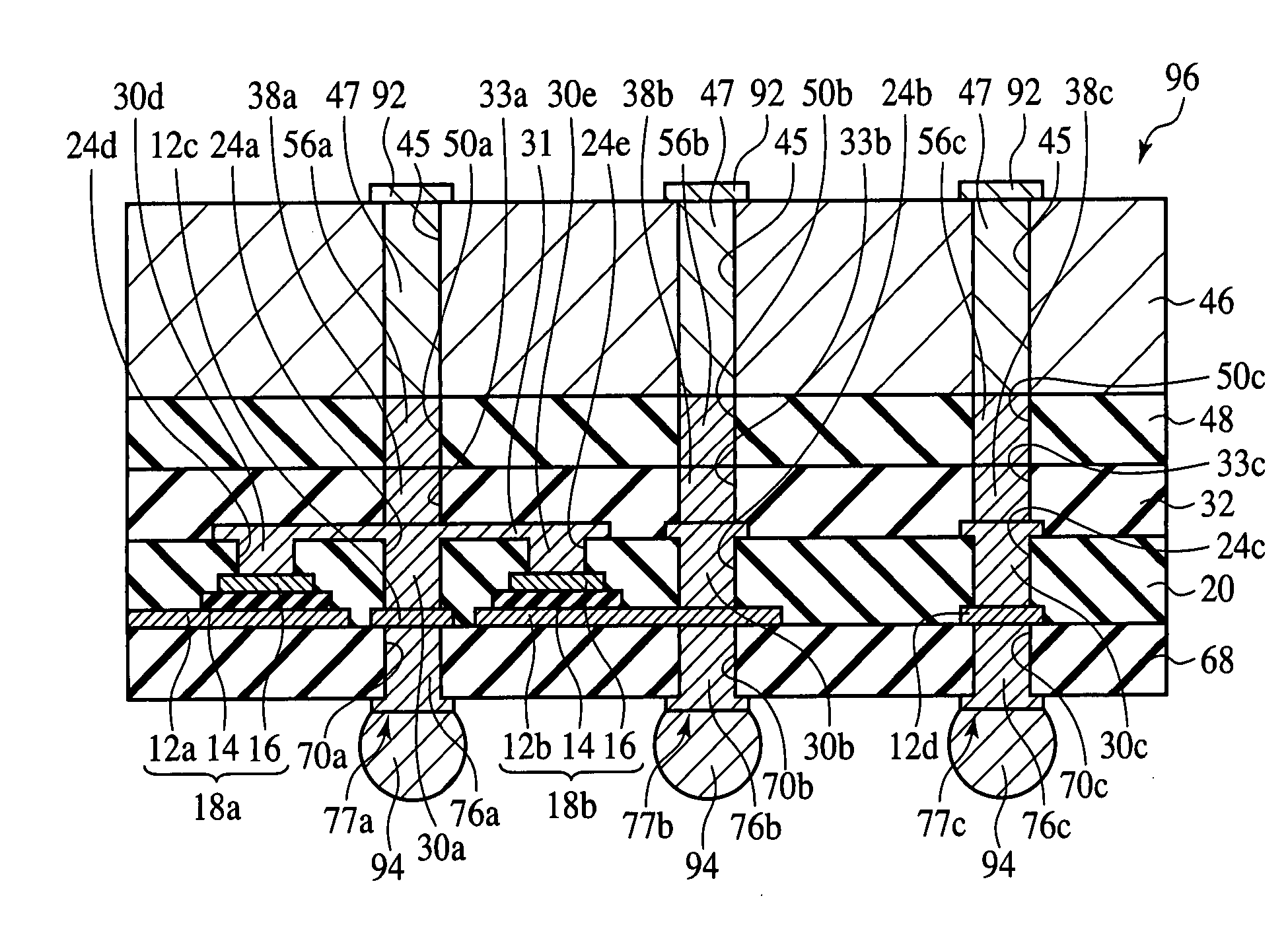
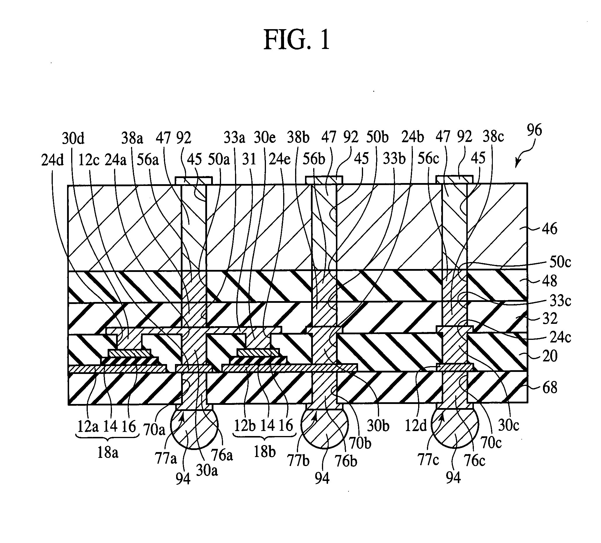
[0060] First, the interposer and the electronic device according to the present embodiment will be explained with reference to FIGS. 1 and 2. FIG. 1 is a sectional view of the interposer according to the present embodiment. FIG. 2 is a sectional view of the electronic device according to the present embodiment.

[0061] As illustrated in FIG. 1, the interposer 96 according to the present embodiment comprises a glass substrate (support substrate) 46 with through-electrodes (vias) 47 buried in, a plurality of resin layers 68, 20, 32 supported by the glass substrate 46 with a resin layer 48 formed therebetween, thin film capacitors 18a, 18b buried in the plu...


PUM

PropertyMeasurementUnit
Dielectric polarization enthalpyaaaaaaaaaa

Abstract

The interposer includes a glass substrate 46 with first through-electrodes 47 buried in; a plurality of resin layers 68, 20, 32 supported by the glass substrate; thin film capacitors 18a, 18b buried between a first resin layer 68 of the plural resin layers and a second resin layer 20 of the plural resin layers and including the first capacitor electrodes 12a, 12b, the second capacitor electrodes 16 opposed to the first capacitor electrodes 12a, 12b, and a dielectric thin film 14 of a relative dielectric constant of 200 or above formed between the first capacitor electrode 12a, 12b and the second capacitor electrode 16, and the second through-electrodes 77a, 77b penetrating the plural resin layers 68, 20, 32, electrically connected to the first through-electrode 47 and electrically connected to the first capacitor electrode 12a, 12b or the second capacitor electrode 16.

Description

CROSS-REFERENCE TO RELATED APPLICATION [0001] This application is based upon and claims priority of Japanese Patent Application No. 2006-260548, filed on Sep. 26, 2006, the contents being incorporated herein by reference. BACKGROUND OF THE INVENTION [0002] The present invention relates to an interposer and a method for manufacturing an interposer, more specifically an interposer including a dielectric thin film of very high dielectric constant, and a method for manufacturing the interposer. [0003] Recently, the digital LSIs (Large Scale Integrated circuits), etc., typically microprocessors have the operation speed increased and the electric power consumption lowered. [0004] In order to operate the LSI in the high-frequency range of the GHz band and at low voltage, it is very important to suppress the power source voltage fluctuation due to abrupt fluctuations of the load impedance, etc. of the LSI while removing high-frequency noises of the power source. [0005] Conventionally, the p...

Claims


Application Information

Patent Timeline
IPC IPC(8): H05K1/16H05K3/30
CPCH05K1/162Y10T29/4913H05K2201/0179H05K2201/09509H05K2201/096H05K2201/09627H05K2201/10378H01L21/486H01L23/15H01L23/498H01L23/49827H01L23/50H01L2224/16H01L2924/01046H01L2924/01077H01L2924/01078H01L2924/01079H01L2924/15311H01L2924/3011H05K1/0306H05K1/112H01L2924/01019H01L2224/16235Y10T29/49002Y10T29/49128Y10T29/49144Y10T29/49155Y10T29/49156H05K3/4605H01L2224/05573H01L2224/05568H01L2924/00014H01L2224/0554H01L2224/05599H01L2224/0555H01L2224/0556
Inventor SHIOGA, TAKESHIKURIHARA, KAZUAKINAKAGAWA, KANAESAKAI, TAIJIMIZUKOSHI, MASATAKA
Owner FUJITSU LTD
Why Eureka
Try Eureka