Method of driving electro-optical element, pixel circuit, electro-optical device, and electronic apparatus

a technology of electrooptical elements and electrooptical devices, applied in the direction of instruments, computing, electric digital data processing, etc., can solve problems such as burn-in and image quality deterioration

Inactive Publication Date: 2008-04-03
JAPAN DISPLAY WEST
View PDF1 Cites 23 Cited by
  • Summary
  • Abstract
  • Description
  • Claims
  • Application Information

AI Technical Summary

Benefits of technology

[0011]An advantage of some aspects of the invention is

Problems solved by technology

When a DC voltage is applied to liquid crystal, image quality deterioration such as burn-in may be caused.
Even in the pixel circuit using the horizontal electric field driving method, since the signals which are image signa

Method used


Image

  • Method of driving electro-optical element, pixel circuit, electro-optical device, and electronic apparatus
  • Method of driving electro-optical element, pixel circuit, electro-optical device, and electronic apparatus
  • Method of driving electro-optical element, pixel circuit, electro-optical device, and electronic apparatus

Examples


first embodiment

1. First Embodiment

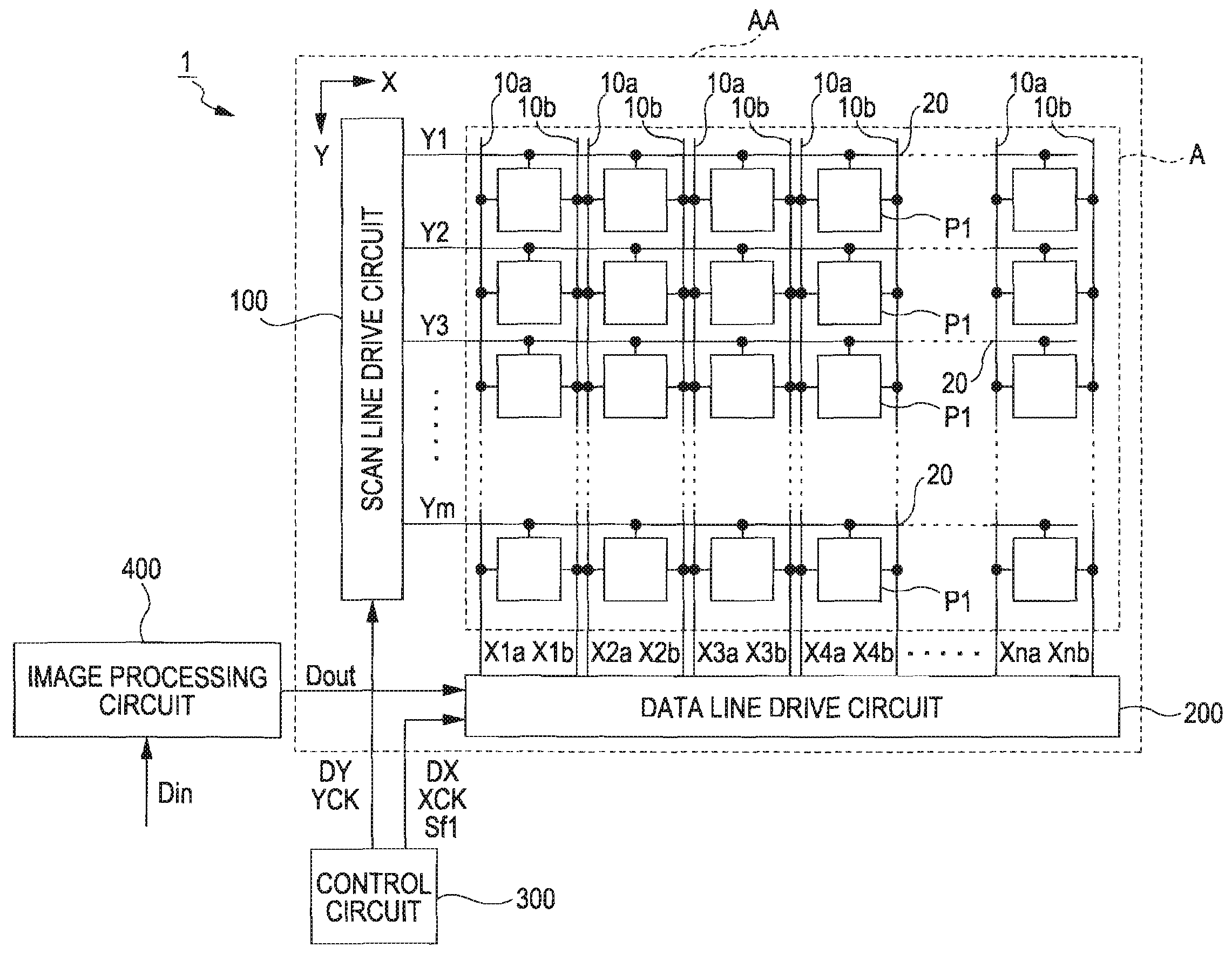
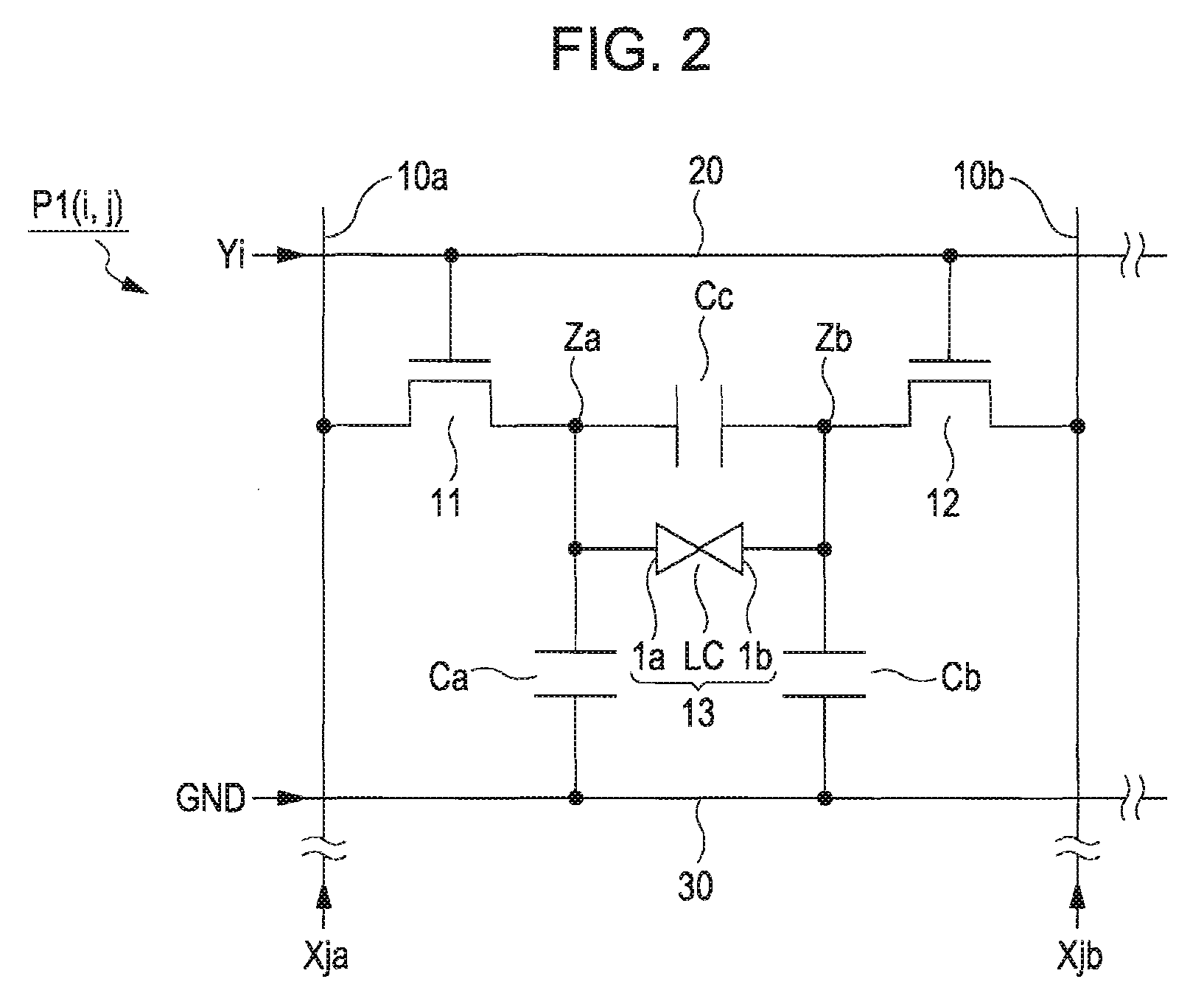
[0048]An electro-optical device according to a first embodiment of the invention uses liquid crystal as an electro-optical material. The electro-optical device 1 has a liquid crystal panel AA (an example of an electro-optical panel) as a main portion. The liquid crystal panel AA is formed by adhering the electrode forming surfaces of a device substrate, on which thin-film transistors (hereinafter, referred to as “TFTs”) are formed as switching elements, and a counter substrate together with a predetermined gap therebetween so that they face each other and inserting liquid crystal into this gap.

[0049]FIG. 1 is a block diagram showing the entire configuration of the electro-optical device 1 according to the first embodiment of the invention. The electro-optical device 1 includes the liquid crystal panel AA, a control circuit 300, and an image processing circuit 400. The liquid crystal display AA is of a transmissive type, but may be of a semi-transmissive type or a ...

second embodiment

2. Second Embodiment

[0088]Next, an electro-optical device according to a second embodiment is equal to the electro-optical device according to the first embodiment shown in FIG. 1, except for the detailed configuration of the image display region A and the detailed configurations of the scan line drive circuit and the data line drive circuit.

[0089]FIG. 9 shows the configuration of the image display region A in the electro-optical device according to the second embodiment. As shown, in the image display region A, pixel circuits P2 arranged in m rows and n columns are formed. In this embodiment, a set of a first scan line 20a and a second scan line 20b is arranged in each row, and n+1 data lines 10ab are arranged in a column direction. First scan signals Y1a to Yma are supplied to m first scan lines 20a and second scan signals Y1b to Ymb are supplied to m second scan lines 20b.

[0090]FIG. 10 is a circuit diagram of a pixel circuit P2(i, j) of the ith row and jth column and a pixel cir...

third embodiment

3. Third Embodiment

[0097]Next, an electro-optical device according to a third embodiment is equal to the electro-optical device according to the first embodiment shown in FIG. 1, except for the detailed configuration of the image display region A and the detailed configurations of the scan line drive circuit and the data line drive circuit.

[0098]FIG. 15 shows the configuration of the image display region A in the electro-optical device according to the third embodiment. As shown, in the image display region A, pixel circuits P3 arranged in m rows and n columns are formed. In this embodiment, a set of a first scan line 20n and a second scan line 20p is arranged in each row, and n first data lines 10a and n second data lines 10b are arranged in a column direction. First scan signals Y1n to Ymn are supplied to m first scan lines 20n and second scan signals Y1p to Ymp are supplied to m second scan lines 20p. In addition, first voltages X1a to Xna are supplied to the n first data lines 1...


PUM


Abstract

Provided is a method of driving an electro-optical element having a first electrode, a second electrode, and an electro-optical material provided between the first electrode and the second electrode and having optical characteristics which vary in accordance with an applied voltage, including: applying a fixed voltage to the first electrode and applying a data voltage according to a gray scale level to be displayed to the second electrode in a first period; applying the data voltage to the first electrode and applying the fixed voltage to the second electrode in a second period; and alternately repeating the driving in the first period and the driving in the second period.

Description

[0001]The entire disclosure of Japanese Patent Application Nos: 2006-214189, filed Aug. 7, 2006 and 2007-152425, filed Jun. 8, 2007 are expressly incorporated by reference herein.BACKGROUND[0002]1. Technical Field[0003]The present invention relates to a technology for driving an electro-optical element such as a liquid crystal element.[0004]2. Related Art[0005]In a liquid crystal device, a driving method in which a vertical electric field is applied in a light emission direction to liquid crystal and a driving method in which a horizontal electric field is applied in a direction perpendicular to the light emission direction to liquid crystal are known. When a DC voltage is applied to liquid crystal, image quality deterioration such as burn-in may be caused. As a driving method, an AC driving method in which an AC voltage is applied to liquid crystal is used.[0006]In a driving method in which a vertical electric field is applied to liquid crystal, for example, a pixel circuit shown i...

Claims


Application Information

Patent Timeline
IPC IPC(8): G09G3/36
CPCG02F1/134363G02F1/136213G09G3/3614G09G3/3659G09G2300/0434G09G2320/0219G09G2300/0842G09G2300/0852G09G2310/0297G09G2320/0204G09G2300/0814G02F1/133G09G3/20G09G3/36
Inventor OZAWA, TOKURO
Owner JAPAN DISPLAY WEST
Why Eureka
Try Eureka