Film-forming system, film-forming method, insulating film, dielectric film, piezoelectric film, ferroelectric film, piezoelectric element and liquid discharge system

a film-forming system and film-forming method technology, applied in the field of film-forming system, film-forming method, insulating film, dielectric film, piezoelectric element and liquid discharge system, can solve problems such as deterioration of film quality, and achieve the effect of high qluality

Inactive Publication Date: 2008-04-03
FUJIFILM CORP
View PDF8 Cites 24 Cited by
  • Summary
  • Abstract
  • Description
  • Claims
  • Application Information

AI Technical Summary

Benefits of technology

[0013] In view of the foregoing observations and description, the primary object of the present invention is to provide a film-forming system and a film-forming process which can optimize the plasma conditions, and form high qluality insulating film or the like having desired characteristics.
[0014] Another object of the present invention is to provide a film-forming system and a film-forming process which can form film in which a perovskite crystal less in the pyrochlore phase can be stably grown.

Problems solved by technology

That is, when the film of sputtering particles is peeled off the shield, it can adhere to the film-forming substrate as particles or impurities, and deteriorate the quality of the film.

Method used


Image

  • Film-forming system, film-forming method, insulating film, dielectric film, piezoelectric film, ferroelectric film, piezoelectric element and liquid discharge system
  • Film-forming system, film-forming method, insulating film, dielectric film, piezoelectric film, ferroelectric film, piezoelectric element and liquid discharge system
  • Film-forming system, film-forming method, insulating film, dielectric film, piezoelectric film, ferroelectric film, piezoelectric element and liquid discharge system

Examples


first embodiment

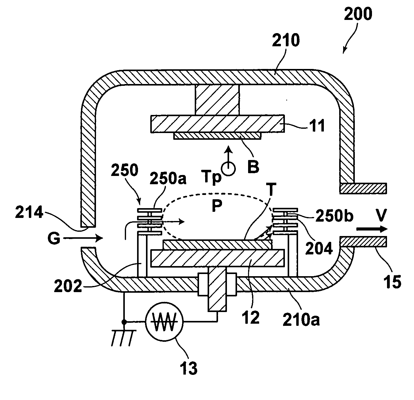
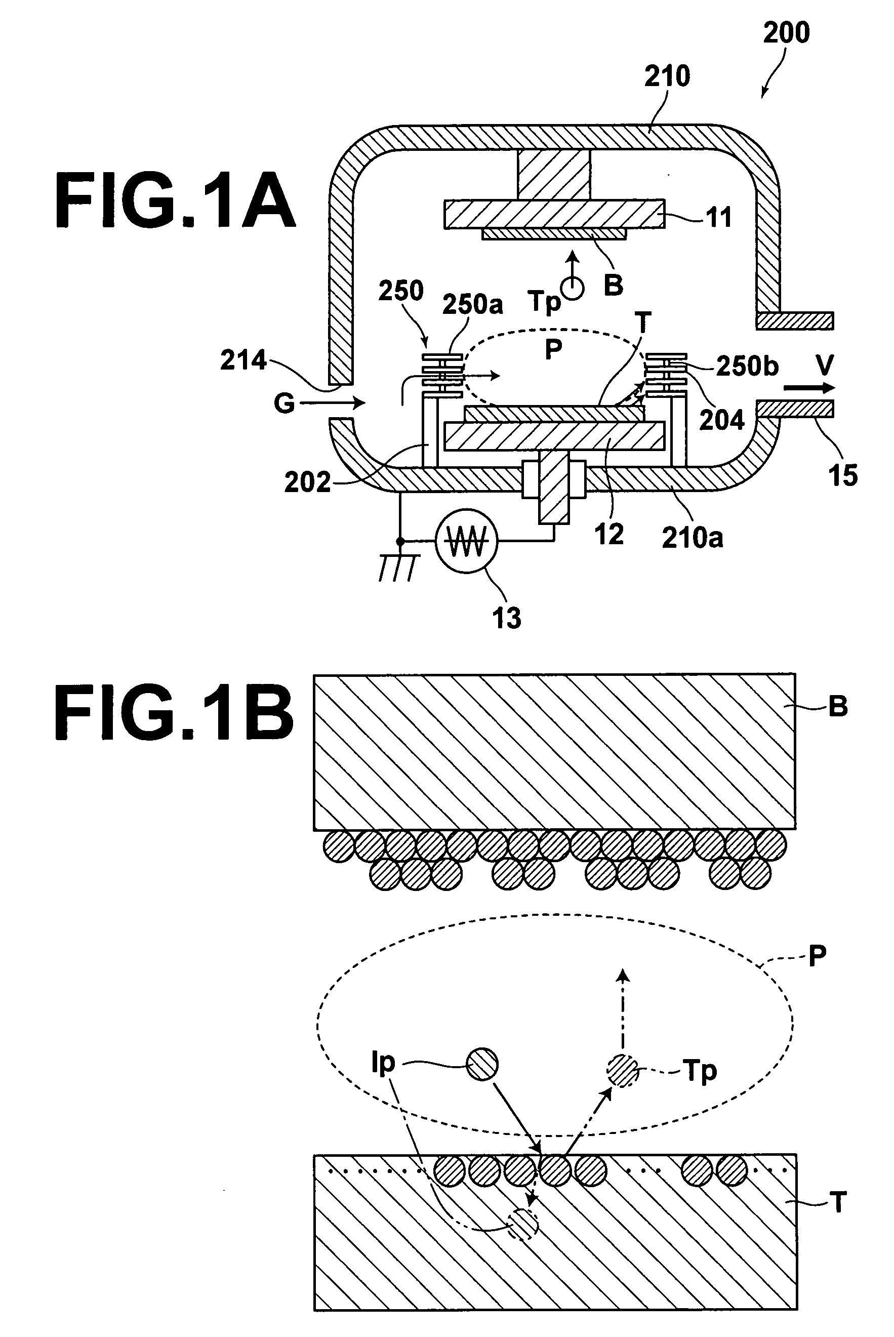
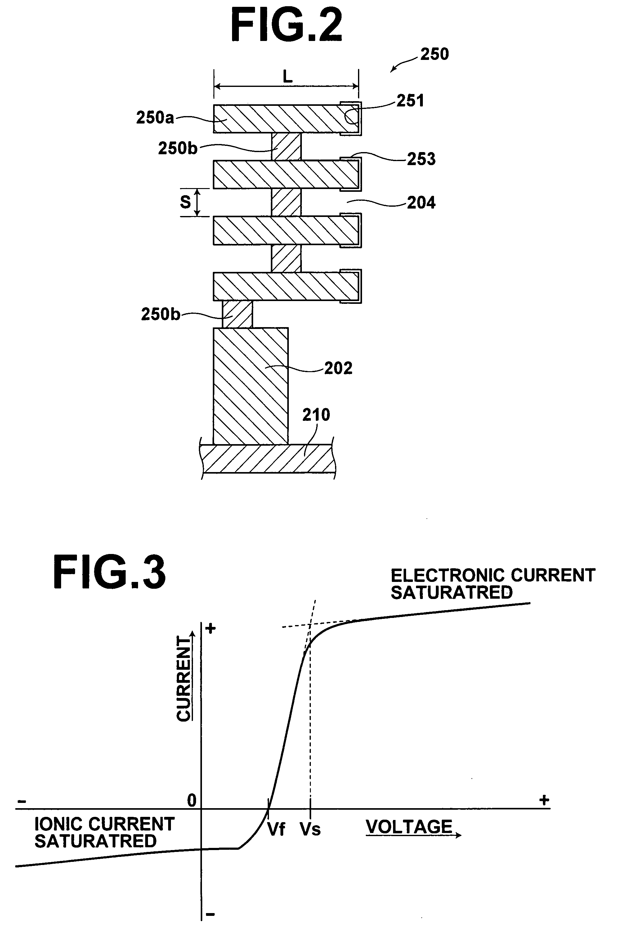
[0058] A first film forming system of the present invention will be described with reference to FIGS. 1A, 1B and 2, hereinbelow. In this embodiment, an RF sputtering system as a film-forming system using plasma will be described with reference to FIGS. 1A and 1B by way example. FIG. 1A is a cross-sectional view showing in brief an RF sputtering system, and FIG. 1B is a schematic view showing formation of film. FIG. 2 is an enlarged view of the shield and the vicinity thereof shown in FIGS. 1A and 1B.

[0059] As shown in FIG. 1A, the film-forming system 200 briefly comprises a vacuum chamber 210 having therein a substrate holder 11 such as an electromagnetic chuck which holds a substrate (film-forming substrate) B and can heat the substrate B to a predetermined temperature and a plasma electrode (cathode electrode) 12 which generates plasma. The plasma electrode 12 corresponds to the target holder which holds a target T.

[0060] The substrate holder 11 and the plasma electrode 12 are s...

second embodiment

[0091] Though, in the embodiment described above, the shield 250 is grounded, the shield 250 may be insulated and applied with a bias voltage. This second embodiment will be described with reference to FIG. 4.

[0092] A film-forming system 300 of this embodiment is shown in FIG. 4 basically the same as the first embodiment except that the shield 250 can be applied with a control voltage. Accordingly, the elements analogous to those in the film-forming system 200 shown in FIG. 1A will be given the same reference numerals and will not be described.

[0093] In this second embodiment, the shield 250 is electrically insulated from the grounded member 202 by way of insulator porcelains 351. The insulator porcelains 351 are similar to the above described spacer 250b, and are disposed in a plurality of sites but differ from the spacer 250b in that the former are insulators. The rings 250a of the shield 250 are laminated together byway of the conductive spacers 250b as in the first embodiment....

examples

[0145] Embodiments of the present invention and comparative examples will be described, hereinbelow.


PUM

PropertyMeasurementUnit
temperatureaaaaaaaaaa
thicknessaaaaaaaaaa
thicknessaaaaaaaaaa

Abstract

A film forming system includes a vacuum chamber introduction and discharge of film-forming gas into and from which are capable. A target holder is disposed in the vacuum chamber to hold a target, a substrate holder is opposed to the target holder and holds a film-forming substrate on which film is formed and a plasma forming portion generates plasma between the target holder and the film-forming substrate. The film-forming system is characterized by having a shield which surrounds the outer peripheral surface of the target holder facing the substrate.

Description

BACKGROUND OF THE INVENTION [0001] 1. Field of the Invention [0002] This invention relates to a system for and a process of forming a film by a vapor phase growth method using plasma; and an insulating film, a dielectric film, a piezoelectric film, a ferroelectric film, a piezoelectric element, and a liquid discharge system formed by the process. [0003] 2. Description of the Related Art [0004] As a method of forming film such as the piezoelectric film there has been known a method where the film is formed by a vapor phase growth method such as sputtering. Sputtering is a method of depositing the component element of a target onto the surface of the substrate by impacting plasma ions such as Ar ions at high energy generated by plasma discharge in high vacuum against the target to release the component elements of the target. [0005] In order to form high quality film, it is necessary to optimize various film-forming conditions. For example, in the piezoelectric film comprising a Pb-co...

Claims


Application Information

Patent Timeline
Patent Type & Authority Applications(United States)
IPC IPC(8): H05H1/24B41J2/14B41J2/16C23C14/08C23C14/34H01L21/316H01L41/09H01L41/18H01L41/187H01L41/316H01L41/39
CPCC23C14/0036C23C14/088C23C14/3407H01J37/32623H01L41/1876H01J37/34H01J37/3447H01L41/316H01J37/32633H10N30/8554H10N30/076
Inventor FUJII, TAKAMICHI
Owner FUJIFILM CORP
Why Eureka
Try Eureka