Eureka AIR delivers breakthrough ideas for toughest innovation challenges, trusted by R&D personnel around the world.

Flash Memory Control Interface

Inactive Publication Date: 2008-04-10
MARVELL WORLD TRADE LTD
View PDF11 Cites 38 Cited by
  • Summary
  • Abstract
  • Description
  • Claims
  • Application Information

AI Technical Summary

Benefits of technology

[0019]In further embodiments, the memory module may further comprise counting logic, the counting logic being configured to compute a unique identifier from a number of clocks between a device configuration command and a corresponding one of the first and second registered signals. Additionally or alternatively, the controller may further comprise configuration logic configured to transmit the configuration signal to the first flash memory device, command control logic configured to transmit a command timing signal to the first and second flash memory devices, timing logic configured to transmit a clock signal to the first and second flash memory devices, and/or a read clo

Problems solved by technology

However a NAND flash I / O interface typically allows only sequential access to data.
Particularly in larger memory structures, such multiple enable pins may result in relatively complicated control logic and consume a relatively large chip area.

Method used


Image

  • Flash Memory Control Interface
  • Flash Memory Control Interface
  • Flash Memory Control Interface

Examples


Embodiment Construction

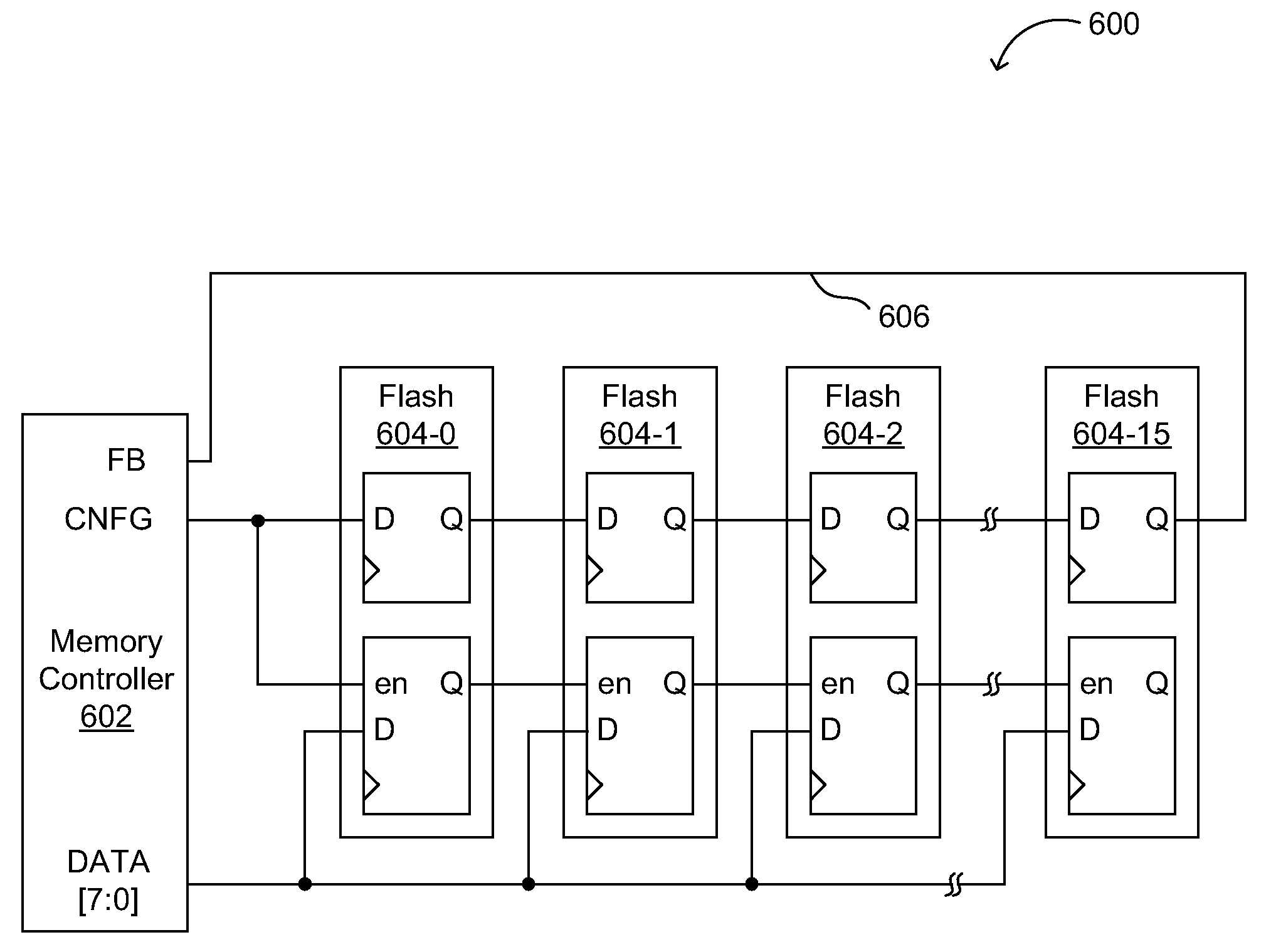
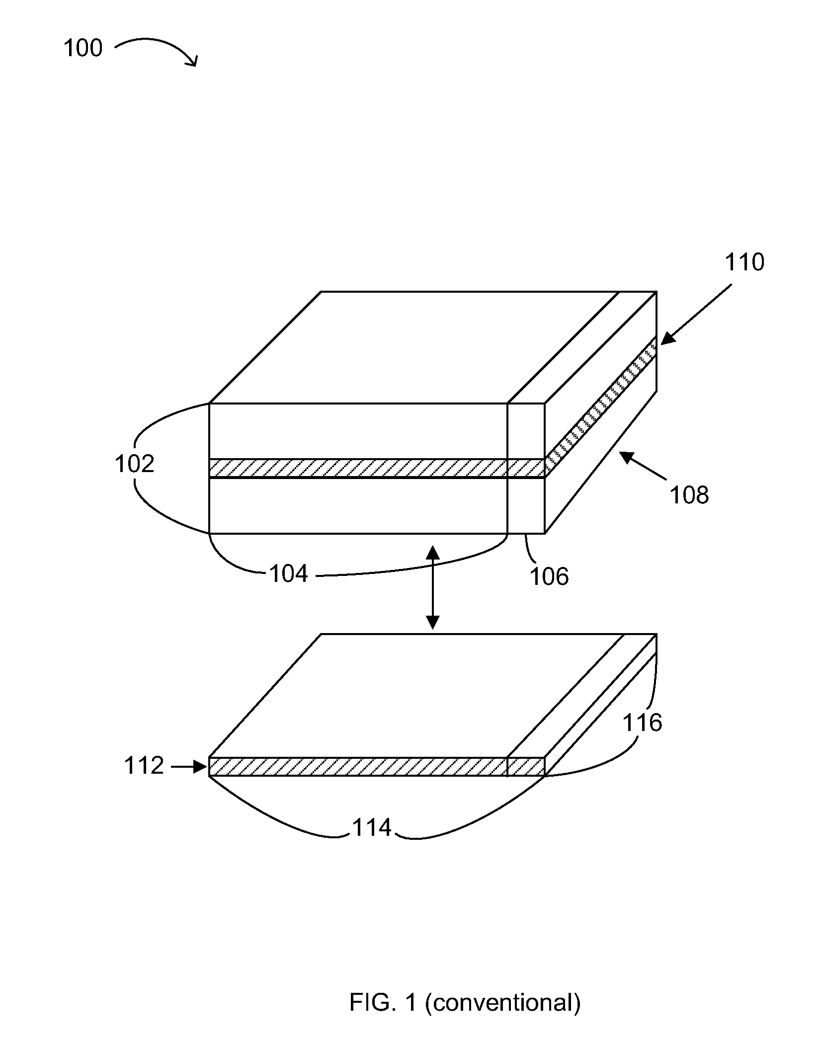
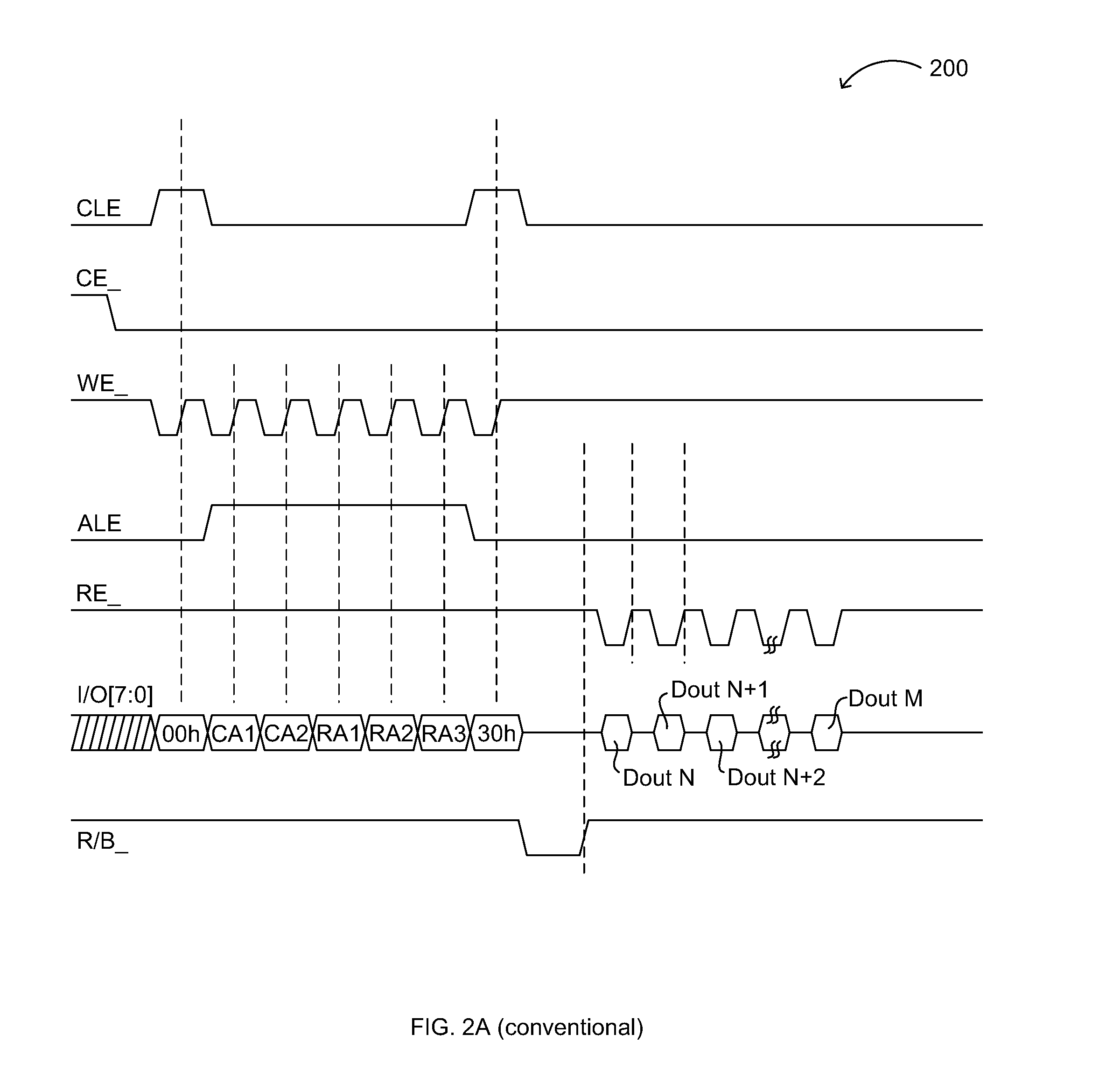
[0034]Reference will now be made in detail to the preferred embodiments of the invention, examples of which are illustrated in the accompanying drawings. While the invention will be described in conjunction with the preferred embodiments, it will be understood that they are not intended to limit the invention to these embodiments. On the contrary, the invention is intended to cover alternatives, modifications, and equivalents that may be included within the spirit and scope of the invention as defined by the appended claims. Furthermore, in the following detailed description of the present invention, numerous specific details are set forth in order to provide a thorough understanding of the present invention. However, it will be readily apparent to one skilled in the art that the present invention may be practiced without these specific details. In other instances, well-known methods, procedures, components, and circuits have not been described in detail so as not to unnecessarily o...


PUM


Abstract

Interfaces, arrangements, and methods for controlling flash memory devices in a multiple device system without increasing the pin count are disclosed. In one embodiment, the system includes first and second flash memory devices and a memory controller. The first memory device receives a configuration signal from a memory controller, and generates a registered signal from the configuration signal for the second memory device. The registered signal may also be provided to the memory controller from a last of the multiple memory devices. The memory controller communicates with the memory devices via an interface that includes a plurality of parallel input / output (I / O) terminals coupled to each of memory device and a serially-connected control terminal. The parallel I / O terminals generally include one or more data I / O terminals configured to transmit data (including parametric data) and commands, a clock terminal configured to receive a clock signal, and a write protect terminal configured to receive a write protection signal.

Description

RELATED APPLICATION(S)[0001]This application claims the benefit of U.S. Provisional Application No. 60 / 798,630 (Attorney Docket No. MP1313PR), filed on Oct. 4, 2006, incorporated herein by reference in its entirety.FIELD OF THE INVENTION[0002]The present invention generally relates to the field of flash memory devices, interfaces and architectures. More specifically, embodiments of the present invention pertain to an interface, arrangement, and method for controlling flash memory devices.DISCUSSION OF THE BACKGROUND[0003]Memory devices, such as flash electrically erasable programmable read only memory (EEPROM), are becoming more widespread. For example, “jump” drives (e.g., for universal serial bus (USB) connections), memory cards, and other nonvolatile memory applications are commonplace in cameras, video games, computers, and other electronic devices. FIG. 1 shows a block diagram of a conventional memory array organization 100. For example, the memory array can be organized in bit...

Claims


Application Information

Patent Timeline
IPC IPC(8): G06F12/02
CPCG06F13/4256G06F13/1668G11C16/34G11C16/10G11C16/26
Inventor URABE, MASAYUKI
Owner MARVELL WORLD TRADE LTD
Why Eureka
Eureka Blog
Learn More