Additive For Copper Plating And Process For Producing Electronic Circiut Substrate Therewith

a technology of additive and copper plating, which is applied in the direction of liquid/solution decomposition chemical coating, organic chemistry, coatings, etc., can solve the problems of difficult quality control in view of practical use, deterioration of film physical properties, and easy degradation of film properties, etc., to achieve easy production, stably fill through holes or via holes for a long time, and extremely easy to handle

Inactive Publication Date: 2008-04-17
EBARA-UDYLITE CO LTD
View PDF4 Cites 18 Cited by
  • Summary
  • Abstract
  • Description
  • Claims
  • Application Information

AI Technical Summary

Benefits of technology

[0023]The additive for copper plating according to the invention can fill through holes or via holes at a micron or sub-micron level even in a case where it comprises one component Accordingly, the copper plating solution using this additive for copper plating can be prepared and handled extremely easily and can stably fill the through holes or via holes for a long time.

Problems solved by technology

Since the ingredient contains a functional group as a cation, it tends to suffer from the effect of a current distribution.
While studies for filling have been progressed based on the combination of properties of each of such ingredients described above, a multi-component additive involves a problem that analysis of them is difficult and the quality control is difficult in view of practical use.
Further, in a case where multi-component additives are present, the concentration of organic materials taken into the plated copper film also increases, which sometimes causes degradation of the film physical property.
It is difficult to completely eliminate the voids or seams, for example, only by current control such as pulse or reverse pulse.

Method used


Image

  • Additive For Copper Plating And Process For Producing Electronic Circiut Substrate Therewith
  • Additive For Copper Plating And Process For Producing Electronic Circiut Substrate Therewith
  • Additive For Copper Plating And Process For Producing Electronic Circiut Substrate Therewith

Examples


example 1

Filling Test for Blind via Hole (1):

[0063]Using as a test specimen an IC substrate having a blind via hole of 65 μm diameter and 60 μm depth (specimen 1) and an IC substrate having a blind via hole of 105 μm diameter and 60 μm depth (specimen 2) , a filling test for the blind via holes treated according to the plating method of the invention was conducted. The composition of the plating solution and the plating conditions are as shown below.

[0064]Copper Sulfate Plating Solution Composition:

Copper sulfate pentahydrate (CuSO4•5H2O):220g / LSulfuric acid (H2SO4):55g / LChlorine ion (Cl−)20mg / LAdditive:Nitrogen-containing biphenyl derivativenote 1)40mg / Lnote 1)In (I), X = formula (III), Y = —OCH3

[0065]Plating Condition:

Cathode current density:0.2425 A / dm2Plating time:200 minPlating solution temperature:25° C.Stirring:Not stirred

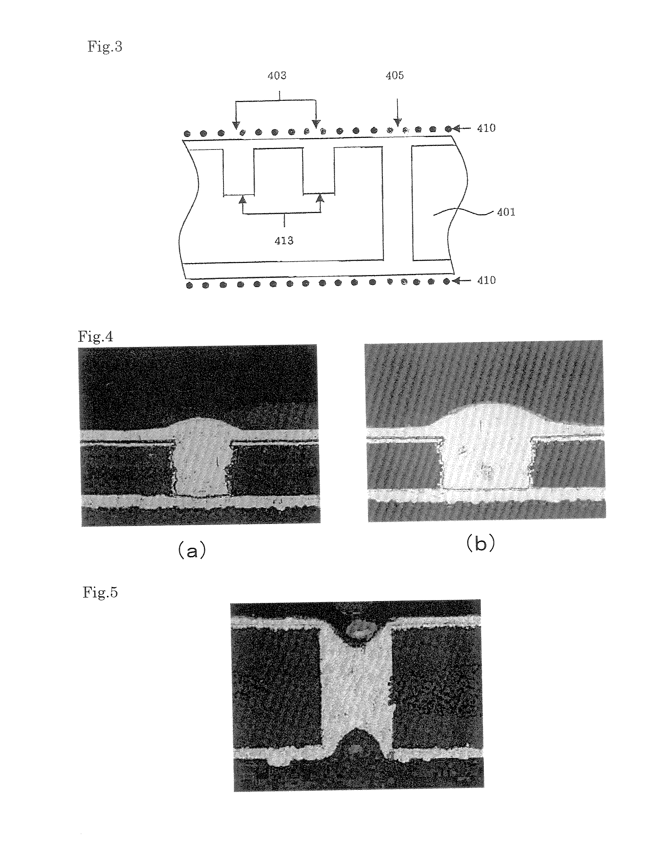
[0066]Cross sectional observation images for the state of the specimen 1 and the specimen 2 after plating are shown in FIG. 4 (a) and FIG. 4(b) As apparent from thes...

example 2

Filling Test for Through Hole:

[0067]Using an IC substrate having through hole of 85 μm diameter and 150 μm depth as a test specimen (specimen 3) a filling test for a through hole treated according to the plating method of the invention was conducted. The composition of the plating solution and the plating conditions are as shown below.

[0068]Copper Sulfate Plating Solution Composition:

Copper sulfate pentahydrate (CuSO4•5H2O):220g / LSulfuric acid (H2SO4):55g / LChlorine ion (Cl−)20mg / LAdditive:Nitrogen-containing biphenyl derivativenote 1)40mg / Lnote 1)Identical with those used in Example 1

[0069]Plating Condition:

Cathode current density:0.2425 A / dm2Plating time:200 minPlating solution temperature:25° C.Stirring:Not stirred

[0070]Cross sectional observation images of the specimen 3 in the state after plating are shown in FIG. 5. A satisfactory through hole filling performance was obtained where the concentration of the nitrogen-containing biphenyl derivative (I) as a single additive was fro...

example 3

Filling Test for Blind via Hole (2)

[0071]Using the specimen 1 (IC substrate having a blind via hole of 65 μm diameter and 60 μm depth) and the specimen 2 (IC substrate having a blind via hole of 105 μm diameter and 60 μm depth) of Example 1, filling tests for the blind via hole were conducted with different plating solutions. The composition of the plating solutions and the plating conditions are as shown below.

[0072]Copper Sulfate Plating Solution Composition:

Copper sulfate pentahydrate (CuSO4•5H2O):220g / LSulfuric acid (H2SO4):55g / LChlorine ion (Cl−)60mg / LAdditive:Nitrogen-containing biphenyl derivative (I)note 2)40mg / LSPSnote 3)0.3mg / Lnote 2)in the formula (I), X = formula (II), Y = —Hnote 3)in the formula (XI), L2 = L3 = —C3H6—, X1 = Y1 = —SO3

[0073]Plating Condition:

Cathode current density and0.97 A / dm2,plating time:30 min → 1.94 A / dm2, 55 minPlating solution temperature:25° C.Stirring:Not stirred

[0074]Cross sectional observation images for the state of the specimen 1 and specime...


PUM

PropertyMeasurementUnit
concentrationaaaaaaaaaa

Abstract

An additive for copper plating comprising, as an effective ingredient, a nitrogen-containing biphenyl derivative represented by the following formula (I):[wherein X represents a group selected from the following groups (II)-(VII):and Y represents a lower alkyl group, lower alkoxy group, nitro group, amino group, sulfonyl group, cyano group, carbonyl group, 1-pyridyl group, or the formula (VIII):(wherein R′ represents a lower alkyl group)], a copper plating solution formed by adding the additive for copper plating to a copper plating solution containing a copper ion ingredient and an anion ingredient, and a method of manufacturing on an electronic circuit substrate having a fine copper wiring circuit, which comprises electroplating in the copper plating solution using as the cathode an electronic circuit substrate in which fine microholes or microgrooves in the shape of an electronic circuit are formed on the surface.The additive for copper plating can fill through holes or via holes at a micron or sub-micron level even in a case where it consists of one component, and the copper plating solution using the additive for copper plating can be prepared and handled extremely easily and can stably fill the through holes or via holes for a long time.

Description

TECHNICAL FIELD[0001]The present invention concerns an additive for copper plating, a copper plating solution containing the same, and a method of manufacturing an electronic circuit substrate using the copper plating solution and, more specifically, it relates to an additive for copper plating capable of filling through holes or blind via holes even upon use of one type of such additive, a copper plating solution containing the same, and a method of manufacturing an electronic circuit substrate such as a semiconductor substrate or a printed circuit substrate (PCB) using the copper plating solution.BACKGROUND ART[0002]Keeping in step with size reductions and diversifications of electronic parts, there has also been demand for decreasing the thickness and decreasing the size of existent semiconductor wafers or IC circuit constituent substrate. Particularly, as Ball Grid Array (BGA) and Chips Scale Packaging (CSP) have come into general use, the size of the IC substrate has decreased ...

Claims


Application Information

Patent Timeline
Patent Type & Authority Applications(United States)
IPC IPC(8): C25D5/02C07D257/04C07D245/02
CPCC07C257/22C07C309/47H05K3/423C07D257/04C25D3/38C07C309/50
Inventor ISHIZUKA, HIROSHISAKAGAWA, NOBUOKIMIZUKA, RYOICHIDOW, WEI-PING
Owner EBARA-UDYLITE CO LTD
Why Eureka
Try Eureka