Semiconductor device and wire bonding method therefor

a technology of semiconductor devices and wire bonding methods, which is applied in the direction of semiconductor devices, semiconductor/solid-state device details, electrical apparatus, etc., can solve the problems of unexpected voids, wire heating and melting, and electric short-circuiting between wires

Inactive Publication Date: 2008-04-17
YAMAHA CORP
View PDF10 Cites 28 Cited by
  • Summary
  • Abstract
  • Description
  • Claims
  • Application Information

AI Technical Summary

Benefits of technology

[0014] It is an object of the present invention to provide a semiconductor device and a wire bonding method therefor, which reliably prevent electric short-circuiting from occurring between adjacent wires connected to leads.
[0015] It is another object of the present invention to provide a wire bonding method that allows large-diameter wires to join bonding pads and contacts having relatively small sizes.
[0016] It is a further object of the present invention to provide semiconductor device using a lead frame and a manufacturing method thereof, which reliably prevents electric short-circuiting from occurring between adjacently positioned wires in proximity to leads.

Problems solved by technology

In this semiconductor device, when electric currents flowing between the electrode pads and leads increase, the wires are heated and melted, or voids unexpectedly occur due to alloy diffusion at joining portions between the wires and leads.
However, the aforementioned constitution has a drawback in that electric short-circuiting may occur between the wires, which are arranged very close to each other within the wires connected to the adjacently arranged leads.

Method used


Image

  • Semiconductor device and wire bonding method therefor
  • Semiconductor device and wire bonding method therefor
  • Semiconductor device and wire bonding method therefor

Examples


first embodiment

1. First Embodiment

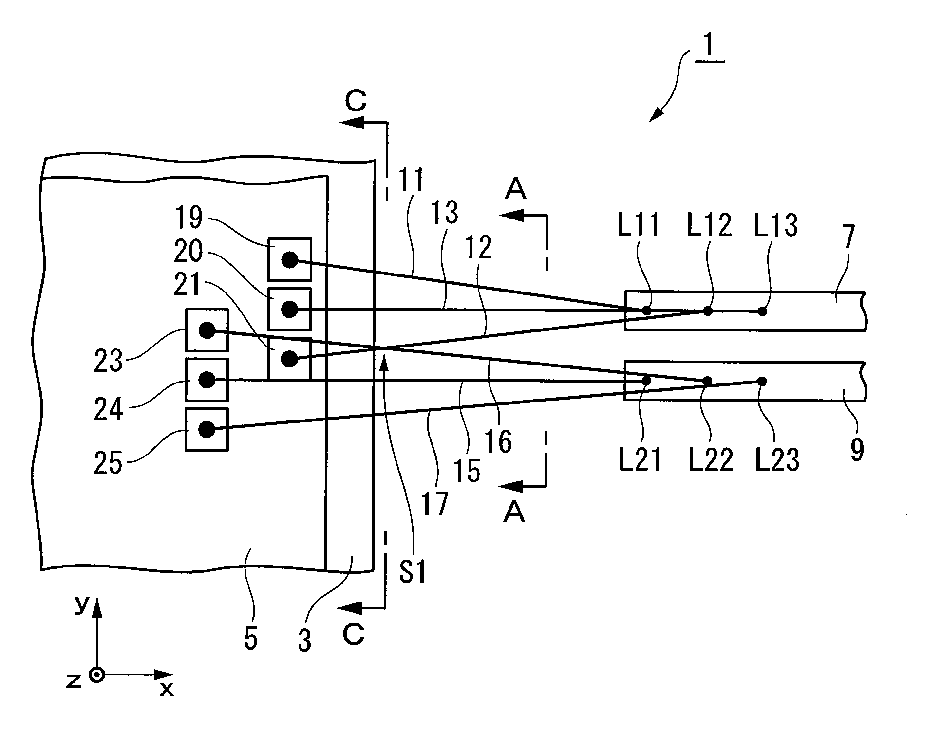
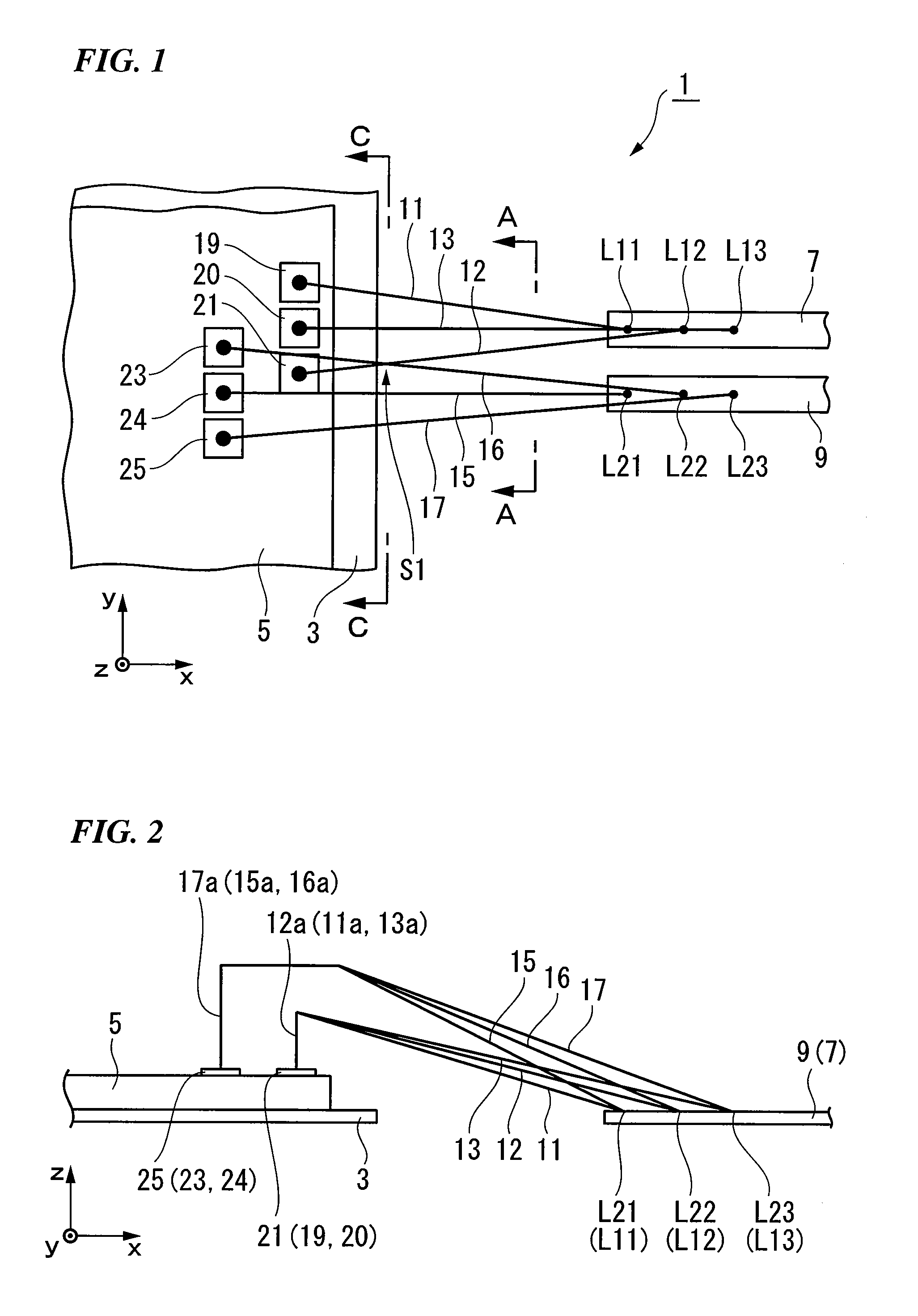
[0070] A semiconductor device 1 according to a first embodiment of the present invention will be described with reference to FIGS. 1 to 4. As shown in FIGS. 1 and 2, a plurality of leads 7 and 9, which are positioned adjacent to each other, are arranged in the periphery of a semiconductor chip 5 mounted on a stage 3 having a planar shape, wherein the lead 7 is electrically connected to three electrode pads 19 to 21 via three wires 11 to 13, and the lead 9 is electrically connected to three electrode pads 23 to 25 via three wires 15 to 17. Plural sets of the lead and three electrodes connected via three wires are arranged for the semiconductor chip 5.

[0071] Each of the leads 7 and 9 has a slender shape elongated toward the semiconductor chip 5. Second bonds L11 to L13 connected to the wires 11 to 13 are aligned in the lead 7 in its longitudinal direction, and second bonds L21 to L23 connected to the wires 15 to 17 are aligned in the lead 9 in its longitudinal dire...

second embodiment

2. Second Embodiment

[0103] Next, a wire bonding method according to a second embodiment of the present invention will be described with reference to FIGS. 7A to 7C, FIGS. 8A and 8B, FIGS. 9A to 9C, FIGS. 10A and 10B, and FIGS. 11A and 11B. As shown in FIGS. 7A-7C, 8A, 8B, 9A, and 9B, the wire bonding method is performed to establish electrical connection between bonding pads 101a formed on a semiconductor chip 101 mounted on a board 103 and electrode pads (or connection pads) 103a formed on the board 103 in the periphery of the semiconductor chip 101 via metal wires 105.

[0104] As shown in FIG. 7A, the semiconductor chip 101 is mounted on the board 103 in advance so that the electrode pads 103a are formed on the board 103 in the periphery of the semiconductor chip 101. Herein, a small-diameter capillary 109 is used to supply thin wires 107 whose diameters are smaller than diameters of the metal wires 105. The terminal end of the small-diameter capillary 109 is pressed onto the elect...

third embodiment

3. Third Embodiment

[0131] A semiconductor device 201 according to a third embodiment of the present invention will be described with reference to FIGS. 12 to 14. As shown in FIGS. 12 and 13, a semiconductor chip 205 is mounted on a surface 203a of a stage 203 having a planar shape in plan view, wherein a plurality of electrode pads 207 and 209 are formed on a surface 205a of the semiconductor chip 205. A plurality of leads 211 and 213 are arranged in the periphery of the semiconductor chip 205, wherein they are connected to the electrode pads 207 and 209 via a plurality of wires 215 and 217.

[0132] In the semiconductor chip 201, the stage 203, the semiconductor chip 205, and the wires 2215 and 217 are sealed with a molded resin 219, which also integrally fixes the stage 203, the semiconductor chip 205, the leads 211 and 213, and the wires 215 and 217 in prescribed positioning.

[0133] The electrode pads 207 and 209 are alternately aligned in different lines on the surface 205a of the...


PUM


Abstract

In a semiconductor device, first wires each having a relatively low loop height are formed between a first lead and a plurality of first electrode pads aligned in a first line, and then second wires each having a relatively high loop height are formed between a second lead and a plurality of second electrode pads aligned in a second line, wherein the second line is distanced from the first line in view of the first and second leads. Wire bonding is sequentially performed so as to increase the height difference between the first wire and the second wire, thus avoiding the occurrence of electric short-circuiting between adjacently arranged wires. In wire bonding, a bump forming process, a ball bonding process, and a wedge bonding process are sequentially performed. It is preferable that the second lead be vertically distanced from the first lead in the thickness direction.

Description

BACKGROUND OF THE INVENTION [0001] 1. Field of the Invention [0002] The present invention relates to semiconductor devices and wire bonding methods therefor. The present invention also relates to manufacturing methods of semiconductor devices using lead frames. [0003] This application claims priority on Japanese Patent Application No. 2006-221457, Japanese Patent Application No. 2006-240005, and Japanese Patent Application No. 2006-280313, the contents of which are incorporated herein by reference. [0004] 2. Description of the Related Art [0005] Japanese Unexamined Patent Application Publication No. H06-302638 teaches an example of a semiconductor device in which bonding wires are arranged so as not to come in contact with each other, wherein electrode pads of a semiconductor chip are each electrically connected to leads arranged in the periphery of the semiconductor chip via wires. In this semiconductor device, when electric currents flowing between the electrode pads and leads inc...

Claims


Application Information

Patent Timeline
Patent Type & Authority Applications(United States)
IPC IPC(8): H01L21/60H01L23/49
CPCH01L21/4842H01L2224/451H01L23/49551H01L24/05H01L24/06H01L24/48H01L24/49H01L24/78H01L24/85H01L2224/04042H01L2224/05554H01L2224/05556H01L2224/05599H01L2224/45015H01L2224/48095H01L2224/48247H01L2224/48465H01L2224/48471H01L2224/48479H01L2224/48483H01L2224/4899H01L2224/49052H01L2224/49109H01L2224/49113H01L2224/49171H01L2224/49431H01L2224/49433H01L2224/78301H01L2224/85051H01L2224/85186H01L2224/85201H01L2224/85205H01L2224/85399H01L2224/85986H01L2924/01005H01L2924/01029H01L2924/01082H01L2924/20752H01L2924/20753H01L2924/00014H01L2924/01006H01L2924/01033H01L23/4952H01L2224/45099H01L2224/48227H01L2924/00H01L24/45H01L2924/181H01L2924/00012H01L2224/4554
Inventor OHKAWA, SHINYA
Owner YAMAHA CORP
Why Eureka
Try Eureka