

Microstrip Antenna And High Frequency Sensor Using Microstrip Antenna
a microstrip antenna and high frequency sensor technology, applied in the direction of resonant antennas, substantially flat resonant elements, radiating element structural forms, etc., can solve the problem of being naturally impossible to use a camera for a toilet device, and achieve the effect of simple structur
- Summary
- Abstract
- Description
- Claims
- Application Information
AI Technical Summary
Benefits of technology
Problems solved by technology
Method used
Image

Examples
second embodiment
[0150]FIG. 9 is a plan view of a microstrip antenna according to the present invention. In FIG. 9 and the subsequent figures, to elements which have substantially the same functions as elements of the embodiment described above, the same reference numerals are affixed; and, in the following, duplicated explanation will be omitted.
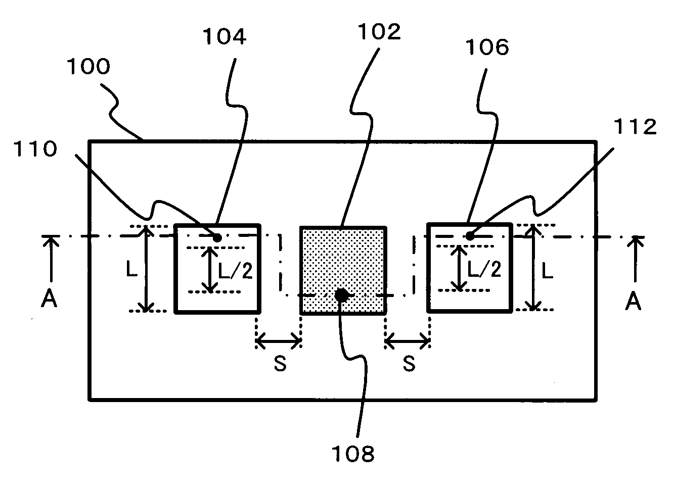
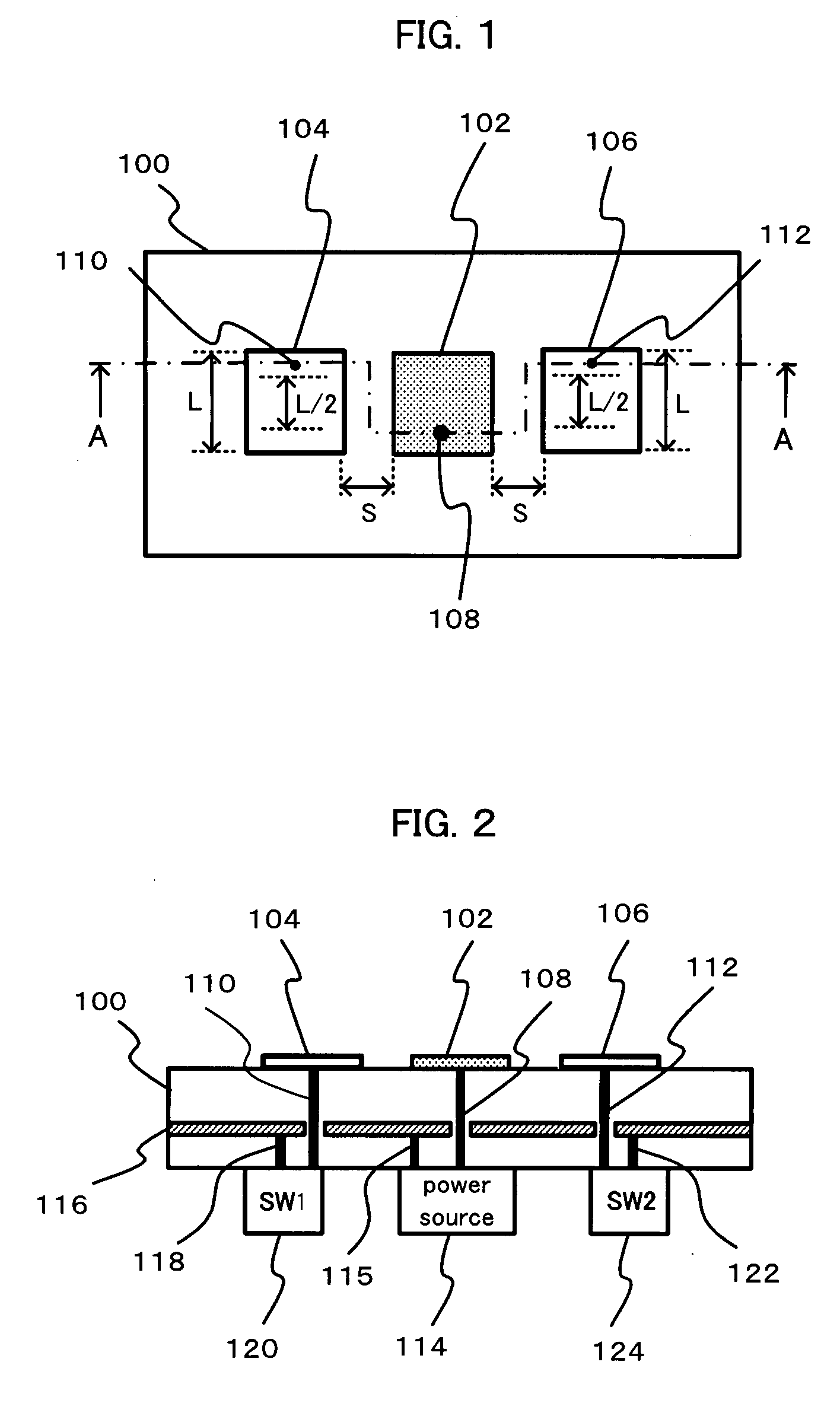
[0151] As shown in FIG. 9, parasitic elements 130 and 132 are provided respectively above and below feed element 102 in the figure. In other words, these three antenna elements 130, 102, and 132 are arranged linearly in the excitating direction of feed element 102 (the vertical direction in the figure). The ground points of these parasitic elements 130 and 132 are at positions further than 0.25 L from the centers of the parasitic elements 130 and 132 in the excitating direction, and control leads 134 and 136, which are through holes, are connected thereto. Although these matters are not shown in the figures, on the rear surface of substrate 100, there are p...
third embodiment
[0154]FIG. 10 is a plan view of a microstrip antenna according to the present invention.
[0155] With the microstrip antenna shown in FIG. 10, in addition to the same structure shown in FIG. 1, outside thereof, there are also appended parasitic elements 140 and 142 on its right and left ends. Respective control leads 144 and 146, which are through holes, are connected to outside parasitic elements 140 and 142 as well. And, by actuation of switches not shown in the figures upon the rear surface of the substrate, it is arranged to switch whether each of these outside parasitic elements 140 and 142 is float, or is grounded. In the figure, reference symbols SW1, SW2, SW3, and SW4 which indicate in the vicinity of the parasitic elements are the name of switches for switching each of the parasitic elements between effective and ineffective (refer to the next FIG. 11).
[0156]FIG. 11 is for the microstrip antenna shown in FIG. 10, and shows the situation in which the radiation angle of the ra...
fourth embodiment
[0162]FIG. 13 is a plan view of a microstrip antenna according to the present invention.
[0163] With this microstrip antenna of FIG. 13, in the same manner as in the case of the structure shown in FIG. 1, along with parasitic elements 104 and 106 being disposed to the right and left of feed element 102 (in other words, on both the sides of feed element 102 in the direction orthogonal to the excitating direction of feed element 102), in the same manner as in the case of the structure shown in FIG. 9, parasitic elements 130 and 132 are also disposed above and below feed element 102 (in other words, on both sides of feed element 102 in the direction along the excitating direction of feed element 102). With regard to a switch structure for switching parasitic elements 104, 106, 130, and 132 between being effective and being ineffective, these are the same as in the case of the embodiments previously described. Reference symbols SW1, SW2, SW3, and SW4 which indicate in the vicinity of the...
PUM
 Abstract
Description
Claims
Application Information