System and method for testing memory blocks in an soc design

a soc design and memory block technology, applied in memory systems, program control, instruments, etc., can solve the problems of design that is not secure, soc does not allow the combination of taps, and cannot read the tap of the soc design

Inactive Publication Date: 2008-04-17
NXP USA INC
View PDF14 Cites 32 Cited by
  • Summary
  • Abstract
  • Description
  • Claims
  • Application Information

AI Technical Summary

Problems solved by technology

This circumvents the problem of generating test vectors for testing memory blocks, since the procedure of generating a set of vectors for a large die area of memory in an SOC chip is complex.
However, the major disadvan...

Method used


Image

  • System and method for testing memory blocks in an soc design
  • System and method for testing memory blocks in an soc design
  • System and method for testing memory blocks in an soc design

Examples


Embodiment Construction

[0010]The detailed description, in connection with the appended drawings, is intended as a description of the presently preferred embodiments of the present invention, and is not intended to represent the only form in which the present invention may be practiced. It is to be understood that the same or equivalent functions may be accomplished by different embodiments that are intended to be encompassed within the spirit and scope of the present invention.

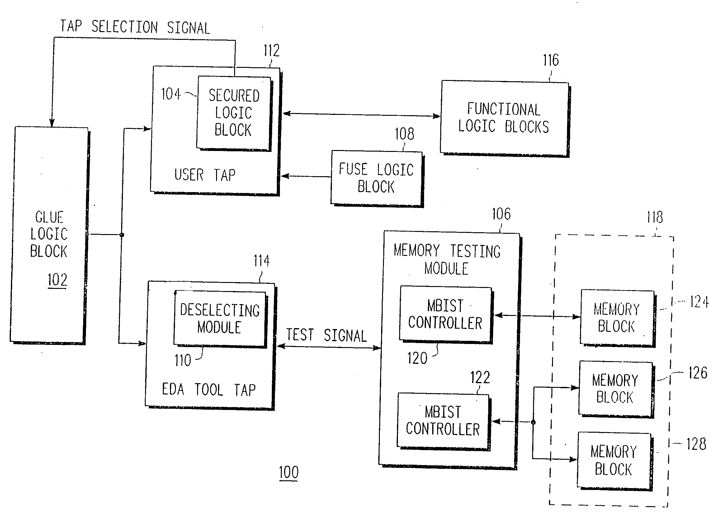
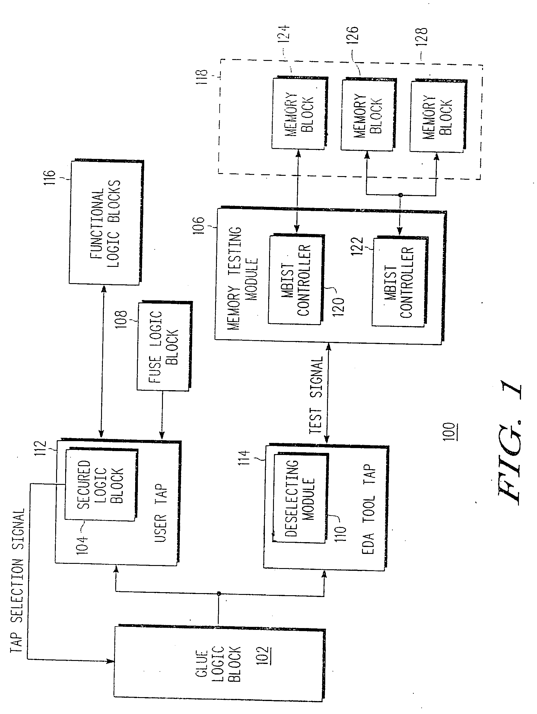
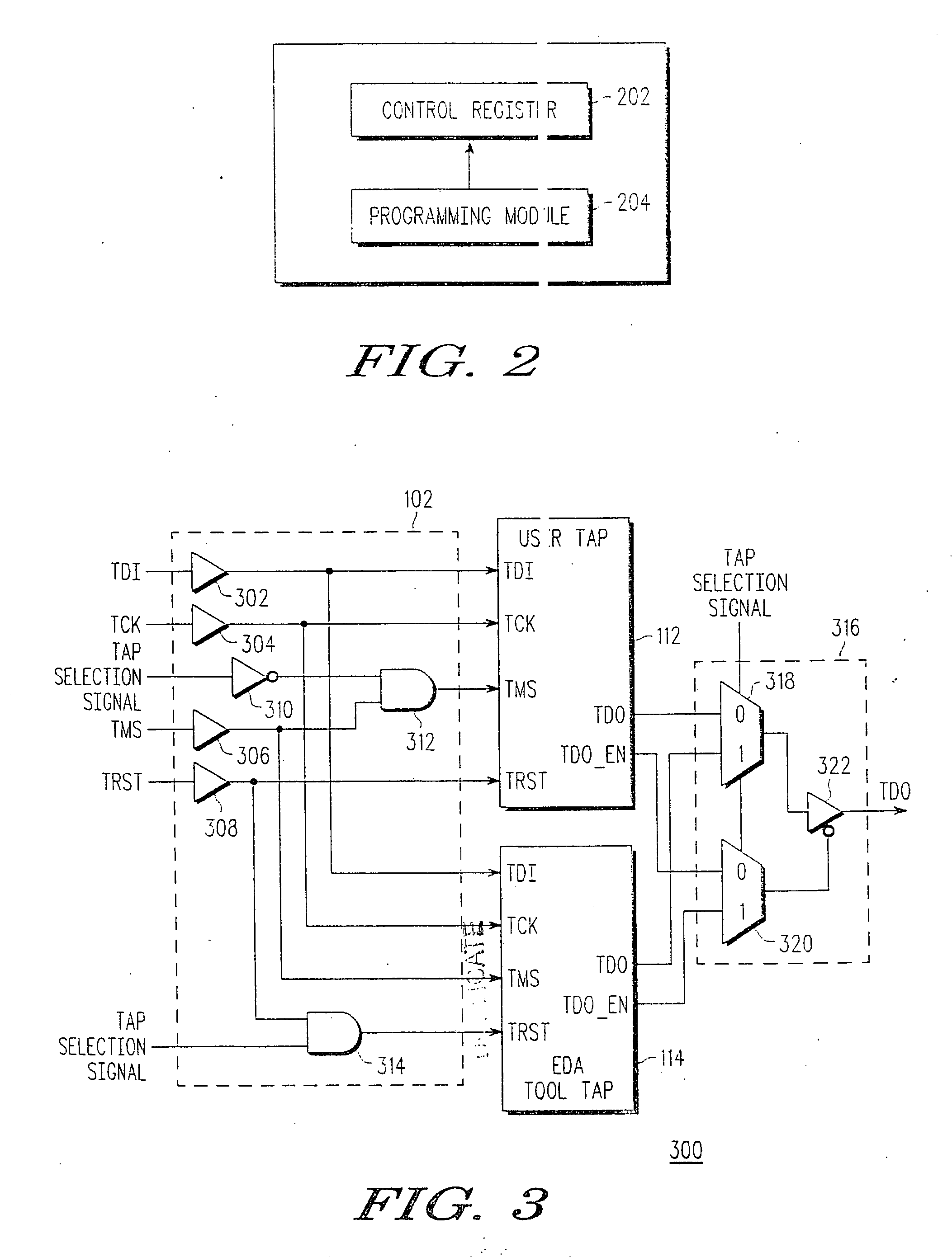
[0011]In an embodiment of the present invention, a system for testing a plurality of memory blocks in a System on Chip (SOC) is provided. The SOC has a number of Test Access Ports (TAPs) including a user TAP and an Electronic Design Automation (EDA) tool TAP. The system includes a glue logic block, a secured logic block, an EDA tool TAP, a fuse logic block, a deselecting module, and a memory testing module. The glue logic block selects the user TAP by default at the outset of a testing phase. The glue logic block selects the EDA too...


PUM


Abstract

A system and method for testing a plurality of memory blocks in a System on Chip (SOC) design uses two Test Access Ports (TAPs), a user TAP and an EDA tool TAP, to provide instructions and test data to the SOC. The system includes a glue logic block, a secured logic block and a memory testing module. The glue logic block selects the user TAP at the outset of the testing phase. The secured logic block is coupled with the user TAP and generates a TAP selection signal, which controls the selection of the EDA tool TAP. The memory testing module is used to carry out the process of testing the memory blocks when the EDA tool TAP is selected.

Description

BACKGROUND OF THE INVENTION[0001]The present invention generally relates to an Integrated Circuit (IC), and more specifically, to a system and method for testing memory blocks in a System on Chip (SOC).[0002]Recently, individual electronic circuits are being integrated onto a single chip, as opposed to having a variety of IC chips being assembled on a circuit board to form a system. These electronic circuits may include functional logic blocks and arrays of memory blocks. In the SOC, the testing and debugging of the functional logic blocks and the arrays of the memory blocks is a matter of major concern.[0003]Currently, boundary-scan testing is a widely used method for testing sub-blocks in an SOC design, since it can be performed without the use of physical test probes. Boundary-scan testing of SOC designs involves boundary-scan signals, known as Test Access Ports (TAPs) signals, being applied through a fixed number of test pins on the SOC. With the acceptance of standard, scan-bas...

Claims


Application Information

Patent Timeline
IPC IPC(8): G01R31/28
CPCG11C29/26G11C29/16
Inventor BAKHSHI, RAKESHDUGGAL, BIPINMIGLANI, GULSHAN KUMAR
Owner NXP USA INC
Why Eureka
Try Eureka