Method for producing group iii - group v vertical light-emitting diodes

a technology of light-emitting diodes and dies, which is applied in the direction of semiconductor/solid-state device manufacturing, semiconductor devices, electrical equipment, etc., can solve the problems of damage to the critical light-emitting active layer, the layer of group iii-n compound semiconductor materials cannot be simply formed with high crystalline quality, and the room for improvemen

Active Publication Date: 2008-05-01
SEMILEDS OPTOELECTRONICS CO LTD
View PDF5 Cites 228 Cited by
  • Summary
  • Abstract
  • Description
  • Claims
  • Application Information

AI Technical Summary

Problems solved by technology

However, layers of Group III-N compound semiconductor materials cannot simply be formed with high crystalline quality on conventional substrates of silicon, germanium, or GaAs, so epitaxial methods were developed using sapphire or silicon carbide (SiC) as a substrate instead.
Even still, the crystallinity and corresponding light emission efficiency of the semiconductor layers produced by these methods leaves room for improvement.
With laser lift-off, however, shockwaves 108 from the laser pulses may travel throughout the LED stack 110 and may damage the critical light-emitting active layer 112.
Furthermore, intentional removal of the GaN or AlGaN buffer layer after removal of the growth-supporting substrate may cause further damage to the device. FIG. 2 is a microscope image 202 and a roughness analysis 204 of the surface of a VLED after removal of a GaN buffer layer.

Method used


Image

  • Method for producing group iii - group v vertical light-emitting diodes
  • Method for producing group iii - group v vertical light-emitting diodes
  • Method for producing group iii - group v vertical light-emitting diodes

Examples


Embodiment Construction

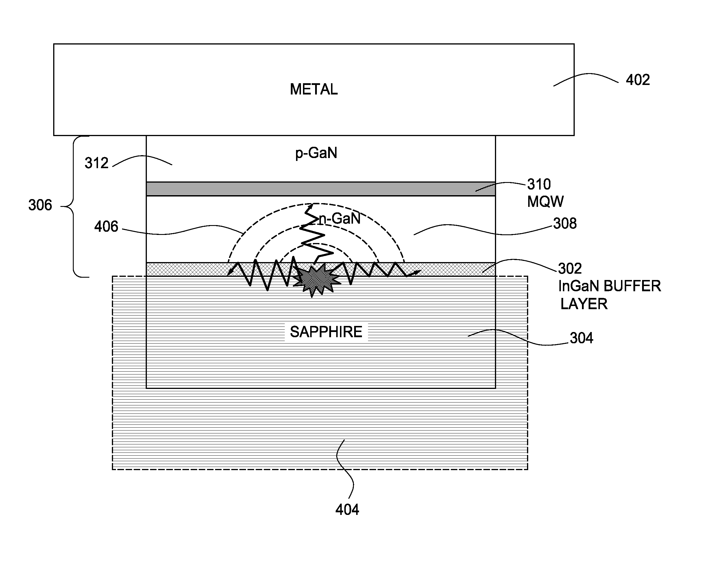
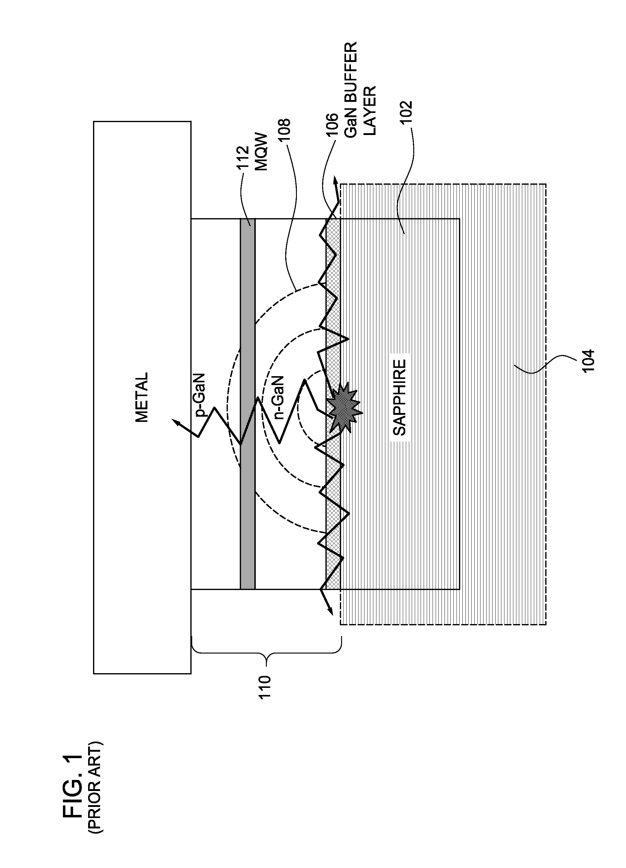
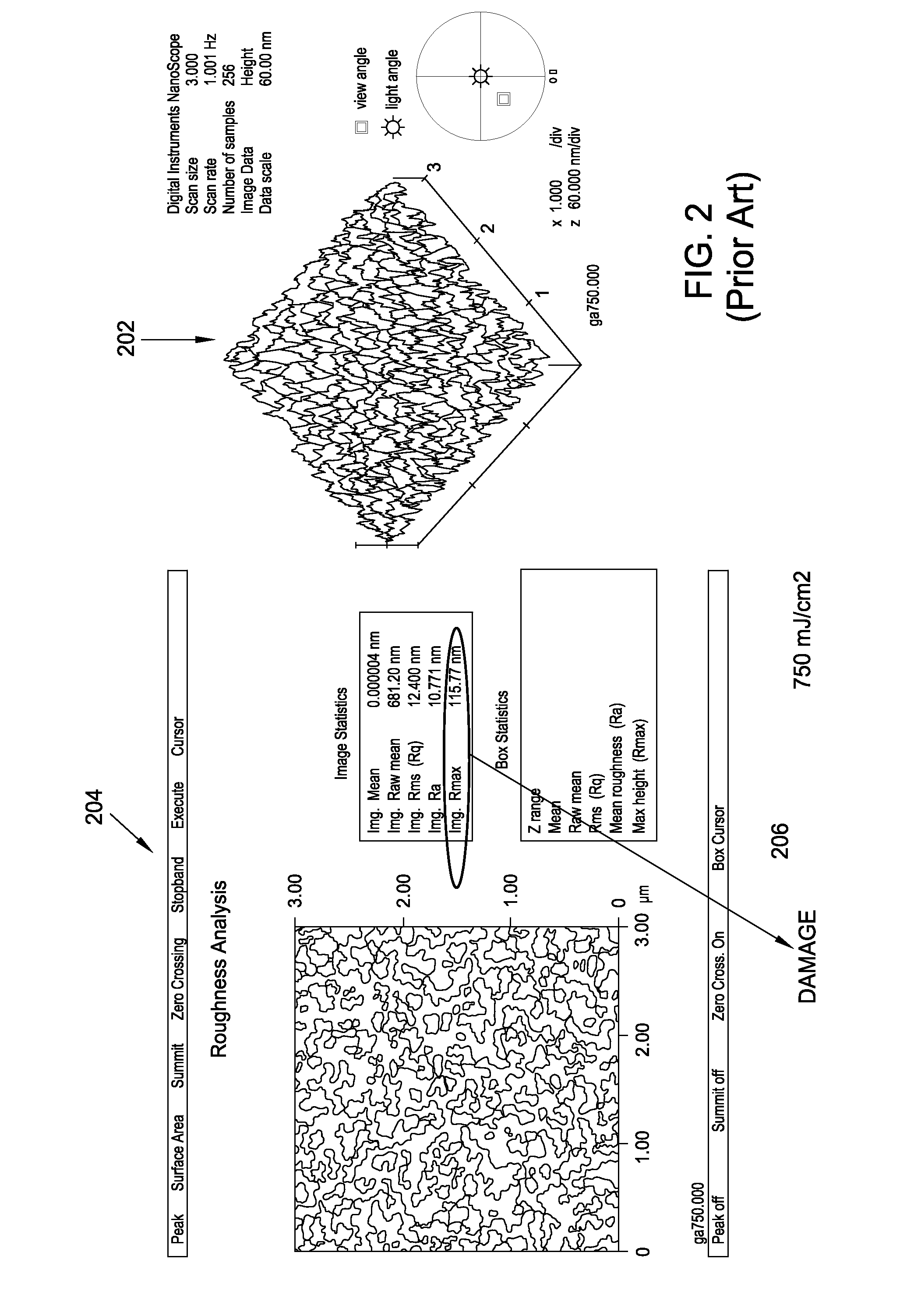
[0025]Embodiments of the invention described herein provide techniques and structures useful for producing one or more vertical light-emitting diode (VLED) dies having a light-emitting diode (LED) stack comprising Group III-Group V (and more particularly, Group III-N) combinations of elements (e.g., GaN, AlN, InN, AlGaN, InGaN, and InAlGaN) and a metal substrate. The techniques include forming an InGaN or InAlGaN interface layer above a suitable growth-supporting substrate, such as sapphire or silicon carbide (SiC), and forming the LED stack above the interface layer. Such an interface layer may absorb a majority of the energy from a laser pulse used during laser lift-off of the growth-supporting substrate in an effort to prevent damage to the light-emitting active layers of the LED stack, which may result in improved brightness performance over VLEDs produced with conventional buffer layers comprising, for example, GaN or AlN.

An Exemplary Interface Layer

[0026]FIG. 3 is a cross-sect...


PUM

PropertyMeasurementUnit
thicknessaaaaaaaaaa
thicknessaaaaaaaaaa
wavelengthaaaaaaaaaa

Abstract

A method of producing one or more vertical light-emitting diode (VLED) dies having a light-emitting diode (LED) stack comprising Group III-Group V combinations of elements (e.g., GaN, AlN, InN, AlGaN, InGaN, and InAlGaN) and a metal substrate is provided. The techniques include forming an InGaN or InAlGaN interface layer above a suitable growth-supporting substrate, such as sapphire or silicon carbide (SiC), and forming the LED stack above the interface layer. Such an interface layer may absorb a majority of the energy from a laser pulse used during laser lift-off of the growth-supporting substrate in an effort to prevent damage to the light emitting layers of the LED stack, which may result in improved brightness performance over VLED dies produced with conventional buffer layers.

Description

BACKGROUND OF THE INVENTION[0001]1. Field of the Invention[0002]Embodiments of the present invention generally relate to light-emitting diode (LED) semiconductor processing and, more particularly, to a method of producing vertical light-emitting diode (VLED) dies comprising Group III-Group V combinations of elements and a metal substrate.[0003]2. Description of the Related Art[0004]To produce blue, green, and ultraviolet vertical light-emitting diodes (VLEDs), various semiconductor materials are utilized, typically comprising combinations of elements from the Group III and Group V areas of the periodic table. Nitrogen being the most prevalent Group V element for such VLEDs, these combinations generally include GaN, AlN, AlGaN, and InGaN. However, layers of Group III-N compound semiconductor materials cannot simply be formed with high crystalline quality on conventional substrates of silicon, germanium, or GaAs, so epitaxial methods were developed using sapphire or silicon carbide (S...

Claims


Application Information

Patent Timeline
Patent Type & Authority Applications(United States)
IPC IPC(8): H01L33/00H01L33/22H01L33/40H01L33/64
CPCH01L33/0079H01L33/641H01L33/405H01L33/22H01L33/0093
Inventor TRAN, ANH CHUONG
Owner SEMILEDS OPTOELECTRONICS CO LTD
Why Eureka
Try Eureka